When people think of wind energy, they usually think of windmill-like turbines dotted among hills or lined up on offshore platforms. But there is also another kind of wind energy, one that replaces stationary, earthbound generators with tethered kites that harvest energy as they soar through the sky.
This airborne form of wind energy, or AWE, is not as well-developed as the terrestrial version, but in principle it has several advantages. Power-generating kites are much less massive than ground-based turbines, which reduces both their production costs and their impact on the landscape. They are also far easier to install in areas that lack well-developed road infrastructure. Finally, and perhaps most importantly, wind speeds are many times greater at high altitudes than they are near the ground, significantly enhancing the power densities available for kites to harvest.
There is, however, one major technical challenge for AWE, and it can be summed up in a single word: control. AWE technology is operationally more complex than conventional turbines, and the traditional method of controlling kites (known as model-predictive control) struggles to adapt to turbulent wind conditions. At best, this reduces the efficiency of energy generation. At worst, it makes it challenging to keep devices safe, stable and airborne.
In a paper published in EPL,Antonio Celani and his colleagues Lorenzo Basile and Maria Grazia Berni of the University of Trieste, Italy, and the Abdus Salam International Centre for Theoretical Physics (ICTP) propose an alternative control method based on reinforcement learning. In this form of machine learning, an agent learns to make decisions by interacting with its environment and receiving feedback in the form of “rewards” for good performance. This form of control, they say, should be better at adapting to the variable and uncertain conditions that power-generating kites encounter while airborne.
What was your motivation for doing this work?
Our interest originated from some previous work where we studied a fascinating bird behaviour called thermal soaring. Many birds, from the humble seagull to birds of prey and frigatebirds, exploit atmospheric currents to rise in the sky without flapping their wings, and then glide or swoop down. They then repeat this cycle of ascent and descent for hours, or even for weeks if they are migratory birds. They’re able to do this because birds are very effective at extracting energy from the atmosphere to turn it into potential energy, even though the atmospheric flow is turbulent, hence very dynamic and unpredictable.
Antonio Celani. (Courtesy: Antonio Celani)
In those works, we showed that we could use reinforcement learning to train virtual birds and also real toy gliders to soar. That got us wondering whether this same approach could be exported to AWE.
When we started looking at the literature, we saw that in most cases, the goal was to control the kite to follow a predetermined path, irrespective of the changing wind conditions. These cases typically used only simple models of atmospheric flow, and almost invariably ignored turbulence.
This is very different from what we see in birds, which adapt their trajectories on the fly depending on the strength and direction of the fluctuating wind they experience. This led us to ask: can a reinforcement learning (RL) algorithm discover efficient, adaptive ways of controlling a kite in a turbulent environment to extract energy for human consumption?
What is the most important advance in the paper?
We offer a proof of principle that it is indeed possible to do this using a minimal set of sensor inputs and control variables, plus an appropriately designed reward/punishment structure that guides trial-and-error learning. The algorithm we deploy finds a way to manoeuvre the kite such that it generates net energy over one cycle of operation. Most importantly, this strategy autonomously adapts to the ever-fluctuating conditions induced by turbulence.
Lorenzo Basile. (Courtesy: Lorenzo Basile)
The main point of RL is that it can learn to control a system just by interacting with the environment, without requiring any a priori knowledge of the dynamical laws that rule its behaviour. This is extremely useful when the systems are very complex, like the turbulent atmosphere and the aerodynamics of a kite.
What are the barriers to implementing RL in real AWE kites, and how might these barriers be overcome?
The virtual environment that we use in our paper to train the kite controller is very simplified, and in general the gap between simulations and reality is wide. We therefore regard the present work mostly as a stimulus for the AWE community to look deeper into alternatives to model-predictive control, like RL.
On the physics side, we found that some phases of an AWE generating cycle are very difficult for our system to learn, and they require a painful fine-tuning of the reward structure. This is especially true when the kite is close to the ground, where winds are weaker and errors are the most punishing. In those cases, it might be a wise choice to use other heuristic, hard-wired control strategies rather than RL.
Finally, in a virtual environment like the one we used to do the RL training in this work, it is possible to perform many trials. In real power kites, this approach is not feasible – it would take too long. However, techniques like offline RL might resolve this issue by interleaving a few field experiments where data are collected with extensive off-line optimization of the strategy. We successfully used this approach in our previous work to train real gliders for soaring.
What do you plan to do next?
We would like to explore the use of offline RL to optimize energy production for a small, real AWE system. In our opinion, the application to low-power systems is particularly relevant in contexts where access to the power grid is limited or uncertain. A lightweight, easily portable device that can produce even small amounts of energy might make a big difference in the everyday life of remote, rural communities, and more generally in the global south.
Since the beginning of radiation therapy, almost all treatments have been delivered with the patient lying on a table while the beam rotates around them. But a resurgence in upright patient positioning is changing that paradigm. Novel radiation accelerators such as proton therapy, VHEE, and FLASH therapy are often too large to rotate around the patient, making access limited. By instead rotating the patient, these previously hard-to-access beams could now become mainstream in the future.
Join leading clinicians and experts as they discuss how this shift in patient positioning is enabling exploration of new treatment geometries and supporting the development of advanced future cancer therapies.
L-R Serdar Charyyev, Eric Deutsch, Bill Loo, Rock Mackie
Novel beams covered and their representative speaker
Serdar Charyyev – Proton Therapy – Clinical Assistant Professor at Stanford University School of Medicine Eric Deutsch – VHEE FLASH – Head of Radiotherapy at Gustave Roussy Bill Loo – FLASH Photons – Professor of Radiation Oncology at Stanford Medicine Rock Mackie – Emeritus Professor at University of Wisconsin and Co-Founder and Chairman of Leo Cancer Care
ZAP-X is a next-generation, cobalt-free, vault-free stereotactic radiosurgery system purpose-built for the brain. Delivering highly precise, non-invasive treatments with exceptionally low whole-brain and whole-body dose, ZAP-X’s gyroscopic beam delivery, refined beam geometry and fully integrated workflow enable state-of-the-art SRS without the burdens of radioactive sources or traditional radiation bunkers.
Theresa Hofman
Theresa Hofman is deputy head of medical physics at the European Radiosurgery Center Munich (ERCM), specializing in stereotactic radiosurgery with the CyberKnife and ZAP‑X systems. She has been part of the ERCM team since 2018 and has extensive clinical experience with ZAP‑X, one of the first centres worldwide to implement the technology in 2021. Since then, the team has treated more than 900 patients with ZAP‑X, and she is deeply involved in both clinical use and evaluation of its planning software.
She holds a master’s degree in physics from Ludwig Maximilian University of Munich, where she authored two first‑author publications on range verification in carbon‑ion therapy. At ERCM, she has published additional first‑author studies on CyberKnife kidney‑treatment accuracy and on comparative planning between ZAP‑X and CyberKnife. She is currently conducting further research on the latest ZAP‑X planning software. Her work is driven by the goal of advancing high‑quality radiosurgery and ensuring the best possible treatment for every patient.
Electrochemical impedance spectroscopy (EIS) provides valuable insights into the physical processes within batteries – but how can these measurements directly inform physics-based models? In this webinar, we present recent work showing how impedance data can be used to extract grouped parameters for physics-based models such as the Doyle–Fuller–Newman (DFN) model or the reduced-order single-particle model with electrolyte (SPMe).
We will introduce PyBaMM (Python Battery Mathematical Modelling), an open-source framework for flexible and efficient battery simulation, and show how our extension, PyBaMM-EIS, enables fast numerical impedance computation for any implemented model at any operating point. We also demonstrate how PyBOP, another open-source tool, performs automated parameter fitting of models using measured impedance data across multiple states of charge.
Battery modelling is challenging, and obtaining accurate fits can be difficult. Our technique offers a flexible way to update model equations and parameterize models using impedance data.
Join us to see how our tools create a smooth path from measurement to model to simulation.
An interactive Q&A session follows the presentation.
Noël Hallemans
Noël Hallemans is a postdoctoral research assistant in engineering science at the University of Oxford, where he previously lectured in mathematics at St Hugh’s College. He earned his PhD in 2023 from the Vrije Universiteit Brussel and the University of Warwick, focusing on frequency-domain, data-driven modelling of electrochemical systems.
His research at the Battery Intelligence Lab, led by Professor David Howey, integrates electrochemical impedance spectroscopy (EIS) with physics-based modelling to improve understanding and prediction of battery behaviour. He also develops multisine EIS techniques for battery characterisation during operation (for example, charging or relaxation).
Julia Sutcliffe (second from the left), Chief Scientific Advisor for the UK’s Department for Business and Trade, visits the NQCC’s experimental facilities on the Harwell Cluster (Courtesy: NQCC)
Ever since the National Quantum Computing Centre was launched five years ago, its core mission has been to accelerate the pathway towards practical adoption of the technology. That has required technical innovation to scale up hardware platforms and create the software tools and algorithms needed to tackle real-world applications, but there has also been a strong focus on engaging with companies to build connections, provide access to quantum resources, and identify opportunities for deriving near-term value from quantum computing.
It makes sense, then, that the NQCC should form the cornerstone of a new Quantum Cluster at the Harwell Campus of Science and Innovation in Oxfordshire. The hope is that the NQCC’s technical expertise and infrastructure, combined with the services and facilities available on the wider Harwell Campus, will provide a magnet for new quantum start-ups as well as overseas companies that are seeking to establish a presence within the UK’s quantum ecosystem.
By accelerating collaboration across government, industry and academia, we will turn research excellence into industrial strength.
“We want to leverage the public investment that has been made into the NQCC to catalyse business growth and attract more investment into the UK’s quantum sector,” said Najwa Sidqi, manager of the Harwell Quantum Cluster, at the official launch event in November. “By accelerating collaboration across government, industry and academia, we will turn research excellence into industrial strength.”
The cluster, which has been ramping up its activities over the last year, is working to ambitious targets. Over the next decade the aim is to incubate at least 100 quantum companies on the Harwell site, create more than 1000 skilled jobs, and generate more than £1 billion of private and public investment. “Our aim is to build the foundations of a globally competitive quantum economy that delivers impact far beyond science and research,” added Sidqi.
Tangible evidence that the approach works is offered by the previous clustering activities on the Harwell Campus, notably the Space Cluster that has expanded rapidly since its launch in 2010. Anchored by the RAL Space national laboratory and bolstered by the presence of ESA and the UK Space Agency, the Space Cluster now comprises more than 100 organizations that range from small start-ups to the UK technology hubs of global heavyweights such as Airbus and Lockheed Martin.
More generally, the survival rate of start-up companies operating on the Harwell site is around 95%, compared with an average of around 50%. “At Harwell there is a high density of innovators sharing the same space, which generates more connections and more ideas,” said Julia Sutcliffe, Chief Scientific Advisor for the UK’s Department for Business and Trade. “It provides an incredible combination of world-class infrastructure and expertise, accelerating the innovation pathway and helping to create a low-risk environment for early-stage businesses and investors.”
The NQCC has already seeded that innovation activity through its early engagement with both quantum companies and end users of the technology. One major initiative has been the testbed programme, which has enabled the NQCC to invest £30m in seven hardware companies to deploy prototype quantum computers on the Harwell Campus. As well as providing access to operational systems based on all of the leading qubit modalities, the testbed programme has also provided an impetus for inward investment and job creation.
One clear example is provided by QuEra Computing, a US-based spin-off from Harvard University and the Massachusetts Institute of Technology that is developing a hardware platform based on neutral atoms. QuEra was one of the companies to win funding through the testbed programme, with the firm setting up a UK-based team to deploy its prototype system on the Harwell Campus. But the company could soon see the benefits of establishing a UK centre for technology development on the site. “Harwell is immensely helpful to us,” said Ed Durking, Corporate Director of QuEra Computing UK. “It’s a nucleus where we enjoy access to world-class talent, vendors, customers, and suppliers.”
On a practical level, establishing its UK headquarters on the Harwell Campus has provided QueEra with easy access to specialist contractors and services for fitting out and its laboratories. In June the company moved into a building that is fully equipped with flexible lab space for R&D and manufacturing, and since then the UK-based team has started to build the company’s most powerful quantum computer at the facility. Longer term, establishing a base within the UK could open the door to new collaborations and funding opportunities for QuEra to further develop its technology, with the company now focused on integrating full error correction into its neutral-atom platform by 2026.
Access to the world-class infrastructure on the Harwell Campus has benefitted the other testbed providers in different ways. For ORCA Computing, a UK company developing and manufacturing photonic quantum computers, the goal was to install a testbed system within Harwell’s high-performance computing centre rather than the NQCC’s experimental labs. “Our focus is to build commercial photonic quantum systems that can be integrated into conventional datacentres, enabling hybrid quantum-classical workflows for real-world applications,” explained Geoff Barnes, Head of Customer Success at ORCA. “Having the NQCC as an expert customer enabled us to demonstrate and validate our capabilities, building the system in our own facility and then deploying it within an operational environment.”
This process provided a valuable learning experience for the ORCA engineers. The experts at Harwell helped them to navigate the constraints of installing equipment within a live datacentre, while also providing practical assistance with the networking infrastructure. Now that the system is up and running, the Harwell site also provides ORCA with an open environment for showcasing its technology to prospective customers. “As well as delivering a testbed system to the NQCC, we can now demonstrate our platform to clients within a real-world setting,” added Barnes. “It has also been a critical step toward commercial deployment on our roadmap, enabling our partners to access our systems remotely for applications development.”
Michael Cuthbert (left), Director of the NQCC, takes Sutcliffe and other visitors on a tour of the national lab (Courtesy: NQCC)
While the NQCC has already played a vital role in supporting companies as they make the transition towards commercialization, the Quantum Cluster has a wider remit to extend those efforts into other quantum technologies, such as sensing and communications, that are already finding real-world applications. It will also have a more specific focus on attracting new investment into the UK, and supporting the growth of companies that are transitioning from the start-up phase to establish larger scale commercial operations.
“In the UK we have traditionally been successful in creating spin-off activities from our strong research base, but it has been more challenging to generate the large capital investments needed to scale businesses in the technology sector,” commented Sidqi. “We want to strengthen that pipeline to ensure that the UK can translate its leadership in quantum research and early-stage innovation into long-term prosperity.”
To accelerate that process the Quantum Cluster announced a strategic partnership with Quantum Exponential, the first UK-based venture capital fund to be entirely focused on quantum technologies. Ian Pearson, the non-executive chairman of the Quantum Exponential, explained that the company is working to generate an investment fund of £100m by the end of 2027 that will support quantum companies as they commercialize their technologies and scale up their businesses. “Now is the time for investment into quantum sector,” said Pearson. “A specialist quantum fund with the expertise needed to analyse and price deals, and to do all the necessary due diligence, will attract more private investment that will help UK companies to grow and scale.”
Around two-thirds of the investments will be directed towards UK-based companies, and as part of the partnership Quantum Exponential will work with the Quantum Cluster to identify and support high-potential quantum businesses within the Harwell Campus. The Quantum Cluster will also play a crucial role in boosting investor confidence – particularly in the unique ability of the Harwell Campus to nurture successful technology businesses – and making connections with international innovation networks to provide UK-based companies with improved access to global markets.
“This new cluster strengthens our national capability and sends a clear signal to global investors that the UK is the place to develop and scale quantum technologies,” commented Michael Cuthbert, Director of the NQCC. “It will help to ensure that quantum innovation delivers benefits not just for science and industry, but for the economy and society as a whole.”
Scaling up The IBS Center for Van der Waals Quantum Solids (IBS-VdWQS) acts as a catalyst for advances in fundamental materials science and condensed-matter physics. The purpose-built facility is colocated on the campus of POSTECH, one of Korea’s leading universities. (Courtesy: IBS)
Our multidisciplinary team aims to create heteroepitaxial van der Waals quantum solids at system scales, where the crystal lattices and symmetries of these novel 2D materials are artificially moulded to atomic precision via epitaxial growth. Over time, we also hope to translate these new solids into quantum device platforms.
Clearly there’s all sorts of exotic materials physics within that remit.
Correct. We form van der Waals heterostructures by epitaxial manipulation of the crystal lattice in diverse, atomically thin 2D materials – for example, 2D heterostructures incorporating graphene, boron nitride or transition-metal dichalcogenides (such as MoS2, WSe2, NbSe2, TaSe2 and so on). Crucially, the material layers are held in place only by weak van der Waals forces and with no dangling chemical bonds in the direction normal to the layers.
These 2D layers can also be laterally “stitched” into hexagonal or honeycomb lattices, with the electronic and atomic motions confined into the atomic layers. Using state-of-the-art epitaxial techniques, our team can then artificially stack these lattices to form a new class of condensed matter with exotic interlayer couplings and emergent electronic, optical and magnetic properties – properties that, we hope, will find applications in next-generation quantum devices.
Moon-Ho Jo “While the focus is very much on basic science, epitaxial scalability is hard-wired into all our lines of enquiry.” (Courtesy: IBS)
The IBS headquarters was established in 2011 as Korea’s first dedicated institute for fundamental science. It’s an umbrella organization coordinating the activity of 38 centres-of-excellence across the physical sciences, life sciences, as well as mathematics and data science. In this way, IBS specializes in long-range initiatives that require large groups of researchers from Korea and abroad.
Our IBS-VdWQS is a catalyst for advances in fundamental materials science and condensed-matter physics, essentially positioned as a central-government-funded research institution in a research-oriented university. Particularly important in this regard is our colocation on the campus of Pohang University of Science and Technology (POSTECH), one of Korea’s leading academic centres, and our adjacency to large-scale facilities like the Pohang Synchrotron Radiation Facility (PAL) and Pohang X-ray free-electron laser (PAL-XFEL). It’s worth noting as well that all the principal investigators (PIs) in our centre hold dual positions as IBS researchers and POSTECH professors.
So IBS is majoring on strategic research initiatives?
Absolutely – and that perspective also underpins our funding model. The IBS-VdWQS was launched in 2022 and is funded by IBS for an initial period through to 2032 (with a series of six-year extensions subject to the originality and impact of our research). As such, we are able to encourage autonomy across our 2D materials programme, giving scientists the academic freedom to pursue questions in basic research without the bureaucracy and overhead of endless grant proposals. Team members know that, with plenty of hard work and creativity, they have everything they need here to do great science and build their careers.
Your core remit is fundamental science, but what technologies could eventually emerge from the IBS-VdWQS research programme?
While the focus is very much on basic science, epitaxial scalability is hard-wired into all our lines of enquiry. In short: we are creating new 2D materials via epitaxial growth and this ultimately opens a pathway to wafer-scale industrial production of van der Waals materials with commercially interesting semiconducting, superconducting or emergent properties in general.
Right now, we are investigating van der Waals semiconductors and the potential integration of MoS2 and WSe2 with silicon for new generations of low-power logic circuitry. On a longer timeline, we are developing new types of high-Tc (around 10 K) van der Waals superconductors for applications in Josephson junctions, which are core building blocks in superconducting quantum computers.
There’s a parallel opportunity in photonic quantum computing, with van der Waals materials shaping up as promising candidates for quantum light-emitters that generate on-demand (deterministic) and highly coherent (indistinguishable) single-photon streams.
Establishing a new research centre from scratch can’t have been easy. How are things progressing?
It’s been a busy three years since the launch of the IBS-VdWQS. The most important task at the outset was centralization – pulling together previously scattered resources, equipment and staff from around the POSTECH campus. We completed the move into our purpose-built facility, next door to the PAL synchrotron light source, at the end of last year and have now established dedicated laboratory areas for the van der Waals Epitaxy Division; Quantum Device and Optics Division; Quantum Device Fabrication Division; and the Imaging and Spectroscopy Division.
One of our front-line research efforts is building a van der Waals Quantum Solid Cluster, an integrated system of multiple instruments connected by ultra-high-vacuum lines to maintain atomically clean surfaces. We believe this advanced capability will allow us to reliably study air-sensitive van der Waals materials and open up opportunities to discover new physics in previously inaccessible van der Waals platforms.
Integrated thinking The IBS-VdWQS hosts an end-to-end research programme spanning advanced fabrication, materials characterization and theoretical studies. From left to right: vapour-phase van der Waals crystal growth; femtosecond laser spectroscopy for studying ultrafast charge, spin and lattice dynamics; and an STM system for investigations of electronic structure and local quantum properties in van der Waals materials. (Courtesy: IBS)
Are there plans to scale the IBS-VdWQS work programme?
Right now, my priority is to promote opportunities for graduate students, postdoctoral researchers and research fellows to accelerate the centre’s expanding research brief. Diversity is strength, so I’m especially keen to encourage more in-bound applications from talented experimental and theoretical physicists in Europe and North America. Our current research cohort comprises 30+ PhD students, seven postdocs (from the US, India, China and Korea) and seven PIs.
Over the next five years, we aim to scale up to 25+ postdocs and research fellows and push out in new directions such as scalable quantum devices. In particular, we are looking for scientists with specialist know-how and expertise in areas like materials synthesis, quantum transport, optical spectroscopy and scanning probe microscopy (SPM) to accelerate our materials research.
How do you support your early-career researchers at IBS-VdWQS?
We are committed to nurturing global early-career talent and provide a clear development pathway from PhD through postdoctoral studies to student research fellow and research fellow/PI. Our current staff PIs have diverse academic backgrounds – materials science, physics, electronic engineering and chemistry – and we therefore allow early-career scientists to have a nominated co-adviser alongside their main PI. This model means research students learn in an integrated fashion that encourages a “multidisciplinarian” mindset – majoring in epitaxial growth, low-temperature electronic devices and optical spectroscopy, say, while also maintaining a watching brief (through their co-adviser) on the latest advances in materials characterization and analysis.
What does success look like at the end of the current funding cycle?
With 2032 as the first milestone year in this budget cycle, we are working to establish a global hub for van der Waals materials science – a highly collaborative and integrated research programme spanning advanced fabrication, materials characterization/analysis and theoretical studies. More capacity, more research infrastructure, more international scientists are all key to delivering our development roadmap for 2D semiconductor and superconductor integration towards scalable, next-generation low-power electronics and quantum computing devices.
Myungchul Oh “We are exploring the microscopic nature of quantum materials and their device applications.” (Courtesy: IBS)
Myungchul Oh joined the IBS-VdWQS in 2023 after a five-year stint as a postdoctoral physicist at Princeton University in the US, where he studied strongly correlated phenomena, superconductivity and topological properties in “twisted” graphene systems.
Recruited as an IBS-POSTECH research fellow, Oh holds dual academic positions: team leader for the quantum-device microscopy investigations at IBS-VdWQS and assistant professor in the semiconductor engineering department at POSTECH.
Van der Waals heterostructures, assembled layer-by-layer from 2D materials, enable precise engineering of quantum properties through the interaction between different atomic layers. By extension, Oh and his colleagues are focused on the development of novel van der Waals systems; their integration into devices via nanofabrication; and the study of electrical, magnetic and topological properties under extreme conditions, where quantum-mechanical effects dominate.
“We are exploring the microscopic nature of quantum materials and their device applications,” Oh explains. “Our research combines novel 2D van der Waals heterostructure device fabrication techniques with cryogenic scanning probe microscopy (SPM) measurements – the latter to access the atomic-scale electronic structure and local physical properties of quantum phases in 2D materials.”
Travis Humble is a research leader who’s thinking big, dreaming bold, yet laser-focused on operational delivery. The long-game? To translate advances in fundamental quantum science into a portfolio of enabling technologies that will fast-track the practical deployment of quantum computers for at-scale scientific, industrial and commercial applications.
Validation came in spades last month when, despite the current turbulence around US science funding, QSC was given follow-on DOE backing of $125 million over five years (2025–30) to create “a new scientific ecosystem” for fault-tolerant, quantum-accelerated high-performance computing (QHPC). In short, QSC will target the critical research needed to amplify the impact of quantum computing through its convergence with leadership-class exascale HPC systems.
“Our priority in Phase II QSC is the creation of a common software ecosystem to host the compilers, programming libraries, simulators and debuggers needed to develop hybrid-aware algorithms and applications for QHPC,” explains Humble. Equally important, QSC researchers will develop and integrate new techniques in quantum error correction, fault-tolerant computing protocols and hybrid algorithms that combine leading-edge computing capabilities for pre- and post-processing of quantum programs. “These advances will optimize quantum circuit constructions and accelerate the most challenging computational tasks within scientific simulations,” Humble adds.
Classical computing, quantum opportunity
At the heart of the QSC programme sits ORNL’s leading-edge research infrastructure for classical HPC, a capability that includes Frontier, the first supercomputer to break the exascale barrier and still one of the world’s most powerful. On that foundation, QSC is committed to building QHPC architectures that take advantage of both quantum computers and exascale supercomputing to tackle all manner of scientific and industrial problems beyond the reach of today’s HPC systems alone.
“Hybrid classical-quantum computing systems are the future,” says Humble. “With quantum computers connecting both physically and logically to existing HPC systems, we can forge a scalable path to integrate quantum technologies into our scientific infrastructure.”
Quantum acceleration ORNL’s current supercomputer, Frontier, was the first high-performance machine to break the exascale barrier. Plans are in motion for a next-generation supercomputer, Discovery, to come online at ORNL by 2028. (Courtesy: Carlos Jones/ORNL, US DOE)
Industry partnerships are especially important in this regard. Working in collaboration with the likes of IonQ, Infleqtion and QuEra, QSC scientists are translating a range of computationally intensive scientific problems – quantum simulations of exotic matter, for example – onto the vendors’ quantum computing platforms, generating excellent results out the other side.
“With our broad representation of industry partners,” notes Humble, “we will establish a common framework by which scientific end-users, software developers and hardware architects can collaboratively advance these tightly coupled, scalable hybrid computing systems.”
It’s a co-development model that industry values greatly. “Reciprocity is key,” Humble adds. “At QSC, we get to validate that QHPC can address real-world research problems, while our industry partners gather user feedback to inform the ongoing design and optimization of their quantum hardware and software.”
Quantum impact
Innovation being what it is, quantum computing systems will continue to trend on an accelerating trajectory, with more qubits, enhanced fidelity, error correction and fault-tolerance key reference points on the development roadmap. Phase II QSC, for its part, will integrate five parallel research thrusts to advance the viability and uptake of QHPC technologies.
The collaborative software effort, led by ORNL’s Vicente Leyton, will develop openQSE, an adaptive, end-to-end software ecosystem for QHPC systems and applications. Yigit Subasi from Los Alamos National Laboratory (LANL) will lead the hybrid algorithms thrust, which will design algorithms that combine conventional and quantum methods to solve challenging problems in the simulation of model materials.
Meanwhile, the QHPC architectures thrust, under the guidance of ORNL’s Chris Zimmer, will co-design hybrid computing systems that integrate quantum computers with leading-edge HPC systems. The scientific applications thrust, led by LANL’s Andrew Sornberger, will develop and validate applications of quantum simulation to be implemented on prototype QHPC systems. Finally, ORNL’s Michael McGuire will lead the thrust to establish experimental baselines for quantum materials that ultimately validate QHPC simulations against real-world measurements.
Longer term, ORNL is well placed to scale up the QHPC model. After all, the laboratory is credited with pioneering the hybrid supercomputing model that uses graphics processing units in addition to conventional central processing units (including the launch in 2012 of Titan, the first supercomputer of this type operating at over 10 petaFLOPS).
“The priority for all the QSC partners,” notes Humble, “is to transition from this still-speculative research phase in quantum computing, while orchestrating the inevitable convergence between quantum technology, existing HPC capabilities and evolving scientific workflows.”
Collaborate, coordinate, communicate
Much like its NQISRC counterparts (which have also been allocated further DOE funding through 2030), QSC provides the “operational umbrella” for a broad-scope collaboration of more than 300 scientists and engineers from 20 partner institutions. With its own distinct set of research priorities, that collective activity cuts across other National Laboratories (Los Alamos and Pacific Northwest), universities (among them Berkeley, Cornell and Purdue) and businesses (including IBM and IQM) to chart an ambitious R&D pathway addressing quantum-state (qubit) resilience, controllability and, ultimately, the scalability of quantum technologies.
“QSC is a multidisciplinary melting pot,” explains Humble, “and I would say, alongside all our scientific and engineering talent, it’s the pooled user facilities that we are able to exploit here at Oak Ridge and across our network of partners that gives us our ‘grand capability’ in quantum science [see box, “Unique user facilities unlock QSC opportunities”]. Certainly, when you have a common research infrastructure, orchestrated as part a unified initiative like QSC, then you can deliver powerful science that translates into real-world impacts.”
Unique user facilities unlock QSC opportunities
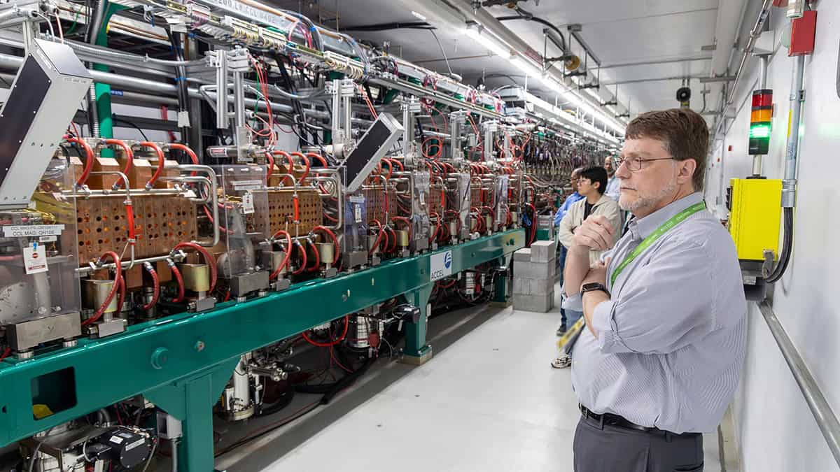
Neutron insights ORNL director Stephen Streiffer tours the linear accelerator tunnel at the Spallation Neutron Source (SNS). QSC scientists are using the SNS to investigate entirely new classes of strongly correlated materials that demonstrate topological order and quantum entanglement. (Courtesy: Alonda Hines/ORNL, US DOE)
Deconstructed, QSC’s Phase I remit (2020–25) spanned three dovetailing and cross-disciplinary research pathways: discovery and development of advanced materials for topological quantum computing (in which quantum information is stored in a stable topological state – or phase – of a physical system rather than the properties of individual particles or atoms); development of next-generation quantum sensors (to characterize topological states and support the search for dark matter); as well as quantum algorithms and simulations (for studies in fundamental physics and quantum chemistry).
Underpinning that collective effort: ORNL’s unique array of scientific user facilities. A case in point is the Spallation Neutron Source (SNS), an accelerator-based neutron-scattering facility that enables a diverse programme of pure and applied research in the physical sciences, life sciences and engineering. QSC scientists, for example, are using SNS to investigate entirely new classes of strongly correlated materials that demonstrate topological order and quantum entanglement – properties that show great promise for quantum computing and quantum metrology applications.
“The high-brightness neutrons at SNS give us access to this remarkable capability for materials characterization,” says Humble. “Using the SNS neutron beams, we can probe exotic materials, recover the neutrons that scatter off of them and, from the resultant signals, infer whether or not the materials exhibit quantum properties such as entanglement.”
While SNS may be ORNL’s “big-ticket” user facility, the laboratory is also home to another high-end resource for quantum studies: the Center for Nanophase Material Science (CNMS), one of the DOE’s five national Nanoscience Research Centers, which offers QSC scientists access to specialist expertise and equipment for nanomaterials synthesis; materials and device characterization; as well as theory, modelling and simulation in nanoscale science and technology.
Thanks to these co-located capabilities, QSC scientists pioneered another intriguing line of enquiry – one that will now be taken forward elsewhere within ORNL – by harnessing so-called quantum spin liquids, in which electron spins can become entangled with each other to demonstrate correlations over very large distances (relative to the size of individual atoms).
In this way, it is possible to take materials that have been certified as quantum-entangled and use them to design new types of quantum devices with unique geometries – as well as connections to electrodes and other types of control systems – to unlock novel physics and exotic quantum behaviours. The long-term goal? Translation of quantum spin liquids into a novel qubit technology to store and process quantum information.
SNS, CNMS and Oak Ridge Leadership Computing Facility (OLCF) are DOE Office of Science user facilities.
When he’s not overseeing the technical direction of QSC, Humble is acutely attuned to the need for sustained and accessible messaging. The priority? To connect researchers across the collaboration – physicists, chemists, material scientists, quantum information scientists and engineers – as well as key external stakeholders within the DOE, government and industry.
“In my experience,” he concludes, ”the ability of the QSC teams to communicate efficiently – to understand each other’s concepts and reasoning and to translate back and forth across disciplinary boundaries – remains fundamental to the success of our scientific endeavours.”
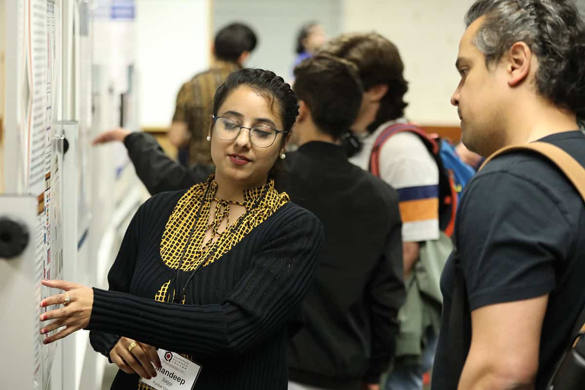
The next generation Quantum science graduate students and postdoctoral researchers present and discuss their work during a poster session at the fifth annual QSC Summer School. Hosted at Purdue University in April this year, the school is one of several workforce development efforts supported by QSC. (Courtesy: Dave Mason/Purdue University)
With an acknowledged shortage of skilled workers across the quantum supply chain, QSC is doing its bit to bolster the scientific and industrial workforce. Front-and-centre: the fifth annual QSC Summer School, which was held at Purdue University in April this year, hosting 130 graduate students (the largest cohort to date) through an intensive four-day training programme.
The Summer School sits as part of a long-term QSC initiative to equip ambitious individuals with the specialist domain knowledge and skills needed to thrive in a quantum sector brimming with opportunity – whether that’s in scientific research or out in industry with hardware companies, software companies or, ultimately, the end-users of quantum technologies in key verticals like pharmaceuticals, finance and healthcare.
“While PhD students and postdocs are integral to the QSC research effort, the Summer School exposes them to the fundamental ideas of quantum science elaborated by leading experts in the field,” notes Vivien Zapf, a condensed-matter physicist at Los Alamos National Laboratory who heads up QSC’s advanced characterization efforts.
“It’s all about encouraging the collective conversation,” she adds, “with lots of opportunities for questions and knowledge exchange. Overall, our emphasis is very much on training up scientists and engineers to work across the diversity of disciplines needed to translate quantum technologies out of the lab into practical applications.”
The programme isn’t for the faint-hearted, though. Student delegates kicked off this year’s proceedings with a half-day of introductory presentations on quantum materials, devices and algorithms. Next up: three and a half days of intensive lectures, panel discussions and poster sessions covering everything from entangled quantum networks to quantum simulations of superconducting qubits.
Many of the Summer School’s sessions were also made available virtually on Purdue’s Quantum Coffeehouse Live Stream on YouTube – the streamed content reaching quantum learners across the US and further afield. Lecturers were drawn from the US National Laboratories, leading universities (such as Harvard and Northwestern) and the quantum technology sector (including experts from IBM, PsiQuantum, NVIDIA and JPMorganChase).
As a theoretical and mathematical physicist at Imperial College London, UK, Bhavin Khatri spent years using statistical physics to understand how organisms evolve. Then the COVID-19 pandemic struck, and like many other scientists, he began searching for ways to apply his skills to the crisis. This led him to realize that the equations he was using to study evolution could be repurposed to model the spread of the virus – and, crucially, to understand how it could be curtailed.
In a paper published in EPL, Khatri models the spread of a SARS-CoV-2-like virus using branching process theory, which he’d previously used to study how advantageous alleles (variations in a genetic sequence) become more prevalent in a population. He then uses this model to assess the duration that interventions such as lockdowns would need to be applied in order to completely eliminate infections, with the strength of the intervention measured in terms of the number of people each infected person goes on to infect (the virus’ effective reproduction number, R).
Tantalizingly, the paper concludes that applying such interventions worldwide in June 2020 could have eliminated the COVID virus by January 2021, several months before the widespread availability of vaccines reduced its impact on healthcare systems and led governments to lift restrictions on social contact. Physics World spoke to Khatri to learn more about his research and its implications for future pandemics.
What are the most important findings in your work?
One important finding is that we can accurately calculate the distribution of times required for a virus to become extinct by making a relatively simple approximation. This approximation amounts to assuming that people have relatively little population-level “herd” immunity to the virus – exactly the situation that many countries, including the UK, faced in March 2020.
Making this approximation meant I could reduce the three coupled differential equations of the well-known SIR model (which models pandemics via the interplay between Susceptible, Infected and Recovered individuals) to a single differential equation for the number of infected individuals in the population. This single equation turned out to be the same one that physics students learn when studying radioactive decay. I then used the discrete stochastic version of exponential decay and standard approaches in branching process theory to calculate the distribution of extinction times.
Simulation trajectories a) A plot of the decline in the number of infected individuals over time. b) Probability density of extinction times for the same parameters as in a), showing that the most likely extinction times are measured in months. (Courtesy: Bhavin S. Khatri 2025 EPL152 11003 DOI 10.1209/0295-5075/ae0c31 CC-BY 4.0 https://creativecommons.org/licenses/by/4.0/)
Alongside the formal theory, I also used my experience in population genetic theory to develop an intuitive approach for calculating the mean of this extinction time distribution. In population genetics, when a mutation is sufficiently rare, changes in its number of copies in the population are dominated by randomness. This is true even if the mutation has a large selective advantage: it has to grow by chance to sufficient critical size – on the order of 1/(selection strength) – for selection to take hold.
The same logic works in reverse when applied to a declining number of infections. Initially, they will decline deterministically, but once they go below a threshold number of individuals, changes in infection numbers become random. Using the properties of such random walks, I calculated an expression for the threshold number and the mean duration of the stochastic phase. These agree well with the formal branching process calculation.
In practical terms, the main result of this theoretical work is to show that for sufficiently strong lockdowns (where, on average, only one of every two infected individuals goes on to infect another person, R=0.5), this distribution of extinction times was narrow enough to ensure that the COVID pandemic virus would have gone extinct in a matter of months, or at most a year.
How realistic is this counterfactual scenario of eliminating SARS-CoV-2 within a year?
Leaving politics and the likelihood of social acceptance aside for the moment, if a sufficiently strong lockdown could have been maintained for a period of roughly six months across the globe, then I am confident that the virus could have been reduced to very low levels, or even made extinct.
The question then is: is this a stable situation? From the perspective of a single nation, if the rest of the world still has infections, then that nation either needs to maintain its lockdown or be prepared to re-impose it if there are new imported cases. From a global perspective, a COVID-free world should be a stable state, unless an animal reservoir of infections causes re-infections in humans.
Modelling the decline of a virus: Theoretical physicist and biologist Bhavin Khatri. (Courtesy: Bhavin Khatri)
As for the practical success of such a strategy, that depends on politics and the willingness of individuals to remain in lockdown. Clearly, this is not in the model. One thing I do discuss, though, is that this strategy becomes far more difficult once more infectious variants of SARS-CoV-2 evolve. However, the problem I was working on before this one (which I eventually published in PNAS) concerned the probability of evolutionary rescue or resistance, and that work suggests that evolution of new COVID variants reduces significantly when there are fewer infections. So an elimination strategy should also be more robust against the evolution of new variants.
What lessons would you like experts (and the public) to take from this work when considering future pandemic scenarios?
I’d like them to conclude that pandemics with similar properties are, in principle, controllable to small levels of infection – or complete extinction – on timescales of months, not years, and that controlling them minimizes the chance of new variants evolving. So, although the question of the political and social will to enact such an elimination strategy is not in the scope of the paper, I think if epidemiologists, policy experts, politicians and the public understood that lockdowns have a finite time horizon, then it is more likely that this strategy could be adopted in the future.
I should also say that my work makes no comment on the social harms of lockdowns, which shouldn’t be minimized and would need to be weighed against the potential benefits.
What do you plan to do next?
I think the most interesting next avenue will be to develop theory that lets us better understand the stability of the extinct state at the national and global level, under various assumptions about declining infections in other countries that adopted different strategies and the role of an animal reservoir.
It would also be interesting to explore the role of “superspreaders”, or infected individuals who infect many other people. There’s evidence that many infections spread primarily through relatively few superspreaders, and heuristic arguments suggest that taking this into account would decrease the time to extinction compared to the estimates in this paper.
I’ve also had a long-term interest in understanding the evolution of viruses from the lens of what are known as genotype phenotype maps, where we consider the non-trivial and often redundant mapping from genetic sequences to function, where the role of stochasticity in evolution can be described by statistical physics analogies. For the evolution of the antibodies that help us avoid virus antigens, this would be a driven system, and theories of non-equilibrium statistical physics could play a role in answering questions about the evolution of new variants.
In proton exchange membrane water electrolysis (PEMWE) systems, voltage cycles dropping below a threshold are associated with reversible performance improvements, which remain poorly understood despite being documented in literature. The distinction between reversible and irreversible performance changes is crucial for accurate degradation assessments. One approach in literature to explain this behaviour is the oxidation and reduction of iridium. Iridium-based electrocatalyst activity and stability in PEMWE hinge on their oxidation state, influenced by the applied voltage. Yet, full-cell PEMWE dynamic performance remains under-explored, with a focus typically on stability rather than activity. This study systematically investigates reversible performance behaviour in PEMWE cells using Ir-black as an anodic catalyst. Results reveal a recovery effect when the low voltage level drops below 1.5 V, with further enhancements observed as the voltage decreases, even with a short holding time of 0.1 s. This reversible recovery is primarily driven by improved anode reaction kinetics, likely due to changing iridium oxidation states, and is supported by alignment between the experimental data and a dynamic model that links iridium oxidation/reduction processes to performance metrics. This model allows distinguishing between reversible and irreversible effects and enables the derivation of optimized operation schemes utilizing the recovery effect.
Tobias Krenz
Tobias Krenz is a simulation and modelling engineer at Siemens Energy in the Transformation of Industry business area focusing on reducing energy consumption and carbon-dioxide emissions in industrial processes. He completed his PhD from Liebniz University Hannover in February 2025. He earned a degree from Berlin University of Applied Sciences in 2017 and a MSc from Technische Universität Darmstadt in 2020.
Alexander Rex
Alexander Rex is a PhD candidate at the Institute of Electric Power Systems at Leibniz University Hannover. He holds a degree in mechanical engineering from Technische Universität Braunschweig, an MEng from Tongji University, and an MSc from Karlsruhe Institute of Technology (KIT). He was a visiting scholar at Berkeley Lab from 2024 to 2025.
Quantum advantage international standardization efforts will, over time, drive economies of scale and multivendor interoperability across the nascent quantum supply chain. (Courtesy: iStock/Peter Hansen)
How do standards support the translation of quantum science into at-scale commercial opportunities?
The standardization process helps to promote the legitimacy of emerging quantum technologies by distilling technical inputs and requirements from all relevant stakeholders across industry, research and government. Put simply: if you understand a technology well enough to standardize elements of it, that’s when you know it’s moved beyond hype and theory into something of practical use for the economy and society.
What are the upsides of standardization for developers of quantum technologies and, ultimately, for end-users in industry and the public sector?
Standards will, over time, help the quantum technology industry achieve critical mass on the supply side, with those economies of scale driving down prices and increasing demand. As the nascent quantum supply chain evolves – linking component manufacturers, subsystem developers and full-stack quantum computing companies – standards will also ensure interoperability between products from different vendors and different regions.
Those benefits flow downstream as well because standards, when implemented properly, increase trust among end-users by defining a minimum quality of products, processes and services. Equally important, as new innovations are rolled out into the marketplace by manufacturers, standards will ensure compatibility across current and next-generation quantum systems, reducing the likelihood of lock-ins to legacy technologies.
What’s your role in coordinating NPL’s standards effort in quantum science and technology?
I have strategic oversight of our core technical programmes in quantum computing, quantum networking, quantum metrology and quantum-enabled PNT (position, navigation and timing). It’s a broad-scope remit that spans research, training as well as responsibility for standardization and international collaboration, with the latter often going hand-in-hand.
Right now, we have over 150 people working within the NPL quantum metrology programme. Their collective focus is on developing the measurement science necessary to build, test and evaluate a wide range of quantum devices and systems. Our research helps innovators, whether in an industry or university setting, to push the limits of quantum technology by providing leading-edge capabilities and benchmarking to measure the performance of new quantum products and services.
Tim Prior “We believe that quantum metrology and standardization are key enablers of quantum innovation.” (Courtesy: NPL)
It sounds like there are multiple layers of activity.
That’s right. For starters, we have a team focusing on the inter-country strategic relationships, collaborating closely with colleagues at other National Metrology Institutes (like NIST in the US and PTB in Germany). A key role in this regard is our standards specialist who, given his background working in the standards development organizations (SDOs), acts as a “connector” between NPL’s quantum metrology teams and, more widely, the UK’s National Quantum Technology Programme and the international SDOs.
We also have a team of technical experts who sit on specialist working groups within the SDOs. Their inputs to standards development are not about NPL’s interests, rather providing expertise and experience gained from cutting-edge metrology; also building a consolidated set of requirements gathered from stakeholders across the quantum community to further the UK’s strategic and technical priorities in quantum.
So NPL’s quantum metrology programme provides a focal point for quantum standardization?
Absolutely. We believe that quantum metrology and standardization are key enablers of quantum innovation, fast-tracking the adoption and commercialization of quantum technologies while building confidence among investors and across the quantum supply chain and early-stage user base. For NPL and its peers, the task right now is to agree on the terminology and best practice as we figure out the performance metrics, benchmarks and standards that will enable quantum to go mainstream.
How does NPL engage the UK quantum community on standards development?
Front-and-centre is the UK Quantum Standards Network Pilot. This initiative – which is being led by NPL – brings together representatives from industry, academia and government to work on all aspects of standards development: commenting on proposals and draft standards; discussing UK standards policy and strategy; and representing the UK in the European and international SDOs. The end-game? To establish the UK as a leading voice in quantum standardization, both strategically and technically, and to ensure that UK quantum technology companies have access to global supply chains and markets.
What about NPL outreach to prospective end-users of quantum technologies?
The Quantum Standards Network Pilot also provides a direct line to prospective end-users of quantum technologies in business sectors like finance, healthcare, pharmaceuticals and energy. What’s notable is that the end-users are often preoccupied with questions that link in one way or another to standardization. For example: how well do quantum technologies stack up against current solutions? Are quantum systems reliable enough yet? What does quantum cost to implement and maintain, including long-term operational costs? Are there other emerging technologies that could do the same job? Is there a solid, trustworthy supply chain?
It’s clear that international collaboration is mandatory for successful standards development. What are the drivers behind the recently announced NMI-Q collaboration?
The quantum landscape is changing fast, with huge scope for disruptive innovation in quantum computing, quantum communications and quantum sensing. Faced with this level of complexity, NMI-Q leverages the combined expertise of the world’s leading National Metrology Institutes – from the G7 countries and Australia – to accelerate the development and adoption of quantum technologies.
No one country can do it all when it comes to performance metrics, benchmarks and standards in quantum science and technology. As such, NMI-Q’s priorities are to conduct collaborative pre-standardization research; develop a set of “best measurement practices” needed by industry to fast-track quantum innovation; and, ultimately, shape the global standardization effort in quantum. NPL’s prominent role within NMI-Q (I am the co-chair along with Barbara Goldstein of NIST) underscores our commitment to evidence-based decision-making in standards development and, ultimately, to the creation of a thriving quantum ecosystem.
What are the attractions of NPL’s quantum programme for early-career physicists?
Every day, our measurement scientists address cutting-edge problems in quantum – as challenging as anything they’ll have encountered previously in an academic setting. What’s especially motivating, however, is that the NPL is a mission-driven endeavour with measurement outcomes linking directly to wider societal and economic benefits – not just in the UK, but internationally as well.
Quantum metrology: at your service
Measurement for Quantum (M4Q) is a flagship NPL programme that provides industry partners with up to 20 days of quantum metrology expertise to address measurement challenges in applied R&D and product development. The service – which is free of charge for projects approved after peer review – helps companies to bridge the gap from technology prototype to full commercialization.
To date, more than two-thirds of the companies to participate in M4Q report that their commercial opportunity has increased as a direct result of NPL support. In terms of specifics, the M4Q offering includes the following services:
Small-current and quantum-noise measurements
Measurement of material-induced noise in superconducting quantum circuits
Nanoscale imaging of physical properties for applications in quantum devices
Characterization of single-photon sources and detectors
Characterization of compact lasers and other photonic components
Semiconductor device characterisation at cryogenic temperatures
“Global collaborations for European economic resilience” is the theme of SEMICON Europa 2025. The event is coming to Munich, Germany on 18–21 November and it will attract 25,000 semiconductor professionals who will enjoy presentations from over 200 speakers.
The TechARENA portion of the event will cover a wide range of technology-related issues including new materials, future computing paradigms and the development of hi-tech skills in the European workface. There will also be an Executive Forum, which will feature leaders in industry and government and will cover topics including silicon geopolitics and the use of artificial intelligence in semiconductor manufacturing.
SEMICON Europa will be held at the Messe München, where it will feature a huge exhibition with over 500 exhibitors from around the world. The exhibition is spread out over three halls and here are some of the companies and product innovations to look out for on the show floor.
Accelerating the future of electro-photonic integration with SmarAct
As the boundaries between electronic and photonic technologies continue to blur, the semiconductor industry faces a growing challenge: how to test and align increasingly complex electro-photonic chip architectures efficiently, precisely, and at scale. At SEMICON Europa 2025, SmarAct will address this challenge head-on with its latest innovation – Fast Scan Align. This is a high-speed and high-precision alignment solution that redefines the limits of testing and packaging for integrated photonics.
Fast Scan Align SmarAct’s high-speed and high-precision alignment solution redefines the limits of testing and packaging for integrated photonics. (Courtesy: SmarAct)
In the emerging era of heterogeneous integration, electronic and photonic components must be aligned and interconnected with sub-micrometre accuracy. Traditional positioning systems often struggle to deliver both speed and precision, especially when dealing with the delicate coupling between optical and electrical domains. SmarAct’s Fast Scan Align solution bridges this gap by combining modular motion platforms, real-time feedback control, and advanced metrology into one integrated system.
At its core, Fast Scan Align leverages SmarAct’s electromagnetic and piezo-driven positioning stages, which are capable of nanometre-resolution motion in multiple degrees of freedom. Fast Scan Align’s modular architecture allows users to configure systems tailored to their application – from wafer-level testing to fibre-to-chip alignment with active optical coupling. Integrated sensors and intelligent algorithms enable scanning and alignment routines that drastically reduce setup time while improving repeatability and process stability.
Fast Scan Align’s compact modules allow various measurement techniques to be integrated with unprecedented possibilities. This has become decisive for the increasing level of integration of complex electro-photonic chips.
Apart from the topics of wafer-level testing and packaging, wafer positioning with extreme precision is as crucial as never before for the highly integrated chips of the future. SmarAct’s PICOSCALE interferometer addresses the challenge of extreme position by delivering picometer-level displacement measurements directly at the point of interest.
When combined with SmarAct’s precision wafer stages, the PICOSCALE interferometer ensures highly accurate motion tracking and closed-loop control during dynamic alignment processes. This synergy between motion and metrology gives users unprecedented insight into the mechanical and optical behaviour of their devices – which is a critical advantage for high-yield testing of photonic and optoelectronic wafers.
Visitors to SEMICON Europa will also experience how all of SmarAct’s products – from motion and metrology components to modular systems and up to turn-key solutions – integrate seamlessly, offering intuitive operation, full automation capability, and compatibility with laboratory and production environments alike.
Optimized pressure monitoring: Efficient workflows with Thyracont’s VD800 digital compact vacuum meters
Thyracont Vacuum Instruments will be showcasing its precision vacuum metrology systems in exhibition hall C1. Made in Germany, the company’s broad portfolio combines diverse measurement technologies – including piezo, Pirani, capacitive, cold cathode, and hot cathode – to deliver reliable results across a pressure range from 2000 to 3e-11 mbar.
VD800 Thryracont’s series combines high accuracy with a highly intuitive user interface, defining the next generation of compact vacuum meters. (Courtesy: Thyracont)
Front-and-centre at SEMICON Europa will be Thyracont’s new series of VD800 compact vacuum meters. These instruments provide precise, on-site pressure monitoring in industrial and research environments. Featuring a direct pressure display and real-time pressure graphs, the VD800 series is ideal for service and maintenance tasks, laboratory applications, and test setups.
The VD800 series combines high accuracy with a highly intuitive user interface. This delivers real-time measurement values; pressure diagrams; and minimum and maximum pressure – all at a glance. The VD800’s 4+1 membrane keypad ensures quick access to all functions. USB-C and optional Bluetooth LE connectivity deliver seamless data readout and export. The VD800’s large internal data logger can store over 10 million measured values with their RTC data, with each measurement series saved as a separate file.
Data sampling rates can be set from 20 ms to 60 s to achieve dynamic pressure tracking or long-term measurements. Leak rates can be measured directly by monitoring the rise in pressure in the vacuum system. Intelligent energy management gives the meters extended battery life and longer operation times. Battery charging is done conveniently via USB-C.
The vacuum meters are available in several different sensor configurations, making them adaptable to a wide range of different uses. Model VD810 integrates a piezo ceramic sensor for making gas-type-independent measurements for rough vacuum applications. This sensor is insensitive to contamination, making it suitable for rough industrial environments. The VD810 measures absolute pressure from 2000 to 1 mbar and relative pressure from −1060 to +1200 mbar.
Model VD850 integrates a piezo/Pirani combination sensor, which delivers high resolution and accuracy in the rough and fine vacuum ranges. Optimized temperature compensation ensures stable measurements in the absolute pressure range from 1200 to 5e-5 mbar and in the relative pressure range from −1060 to +340 mbar.
The model VD800 is a standalone meter designed for use with Thyracont’s USB-C vacuum transducers, which are available in two models. The VSRUSB USB-C transducer is a piezo/Pirani combination sensor that measures absolute pressure in the 2000 to 5.0e-5 mbar range. The other is the VSCUSB USB-C transducer, which measures absolute pressures from 2000 down to 1 mbar and has a relative pressure range from -1060 to +1200 mbar. A USB-C cable connects the transducer to the VD800 for quick and easy data retrieval. The USB-C transducers are ideal for hard-to-reach areas of vacuum systems. The transducers can be activated while a process is running, enabling continuous monitoring and improved service diagnostics.
With its blend of precision, flexibility, and ease of use, the Thyracont VD800 series defines the next generation of compact vacuum meters. The devices’ intuitive interface, extensive data capabilities, and modern connectivity make them an indispensable tool for laboratories, service engineers, and industrial operators alike.
To experience the future of vacuum metrology in Munich, visit Thyracont at SEMICON Europa hall C1, booth 752. There you will discover how the VD800 series can optimize your pressure monitoring workflows.
At-scale quantum By integrating Delft Circuits’ Cri/oFlex® cabling technology (above) into Bluefors’ dilution refrigerators, the vendors’ combined customer base will benefit from an industrially proven and fully scalable I/O solution for their quantum systems. Cri/oFlex® cabling combines fully integrated filtering with a compact footprint and low heatload. (Courtesy: Delft Circuits)
Better together. That’s the headline take on a newly inked technology partnership between Bluefors, a heavyweight Finnish supplier of cryogenic measurement systems, and Delft Circuits, a Dutch manufacturer of specialist I/O cabling solutions designed for the scale-up and industrial deployment of next-generation quantum computers.
The drivers behind the tie-up are clear: as quantum systems evolve – think vastly increased qubit counts plus ever-more exacting requirements on gate fidelity – developers in research and industry will reach a point where current coax cabling technology doesn’t cut it anymore. The answer? Collaboration, joined-up thinking and product innovation.
In short, by integrating Delft Circuits’ Cri/oFlex® cabling technology into Bluefors’ dilution refrigerators, the vendors’ combined customer base will benefit from a complete, industrially proven and fully scalable I/O solution for their quantum systems. The end-game: to overcome the quantum tech industry’s biggest bottleneck, forging a development pathway from quantum computing systems with hundreds of qubits today to tens of thousands of qubits by 2030.
Joined-up thinking
For context, Cri/oFlex® cryogenic RF cables comprise a stripline (a type of transmission line) based on planar microwave circuitry – essentially a conducting strip encapsulated in dielectric material and sandwiched between two conducting ground planes. The use of the polyimide Kapton® as the dielectric ensures Cri/oFlex® cables remain flexible in cryogenic environments (which are necessary to generate quantum states, manipulate them and read them out), with silver or superconducting NbTi providing the conductive strip and ground layer. The standard product comes as a multichannel flex (eight channels per flex) with a range of I/O channel configurations tailored to the customer’s application needs, including flux bias lines, microwave drive lines, signal lines or read-out lines.
“Together with Bluefors, we will accelerate the journey to quantum advantage,” says Robby Ferdinandus of Delft Circuits. (Courtesy: Delft Circuits)
“Reliability is a given with Cri/oFlex®,” says Robby Ferdinandus, global chief commercial officer for Delft Circuits and a driving force behind the partnership with Bluefors. “By integrating components such as attenuators and filters directly into the flex,” he adds, “we eliminate extra parts and reduce points of failure. Combined with fast thermalization at every temperature stage, our technology ensures stable performance across thousands of channels, unmatched by any other I/O solution.”
Technology aside, the new partnership is informed by a “one-stop shop” mindset, offering the high-density Cri/oFlex® solution pre-installed and fully tested in Bluefors cryogenic measurement systems. For the end-user, think turnkey efficiency: streamlined installation, commissioning, acceptance and, ultimately, enhanced system uptime.
Scalability is front-and-centre too, thanks to Delft Circuits’ pre-assembled and tested side-loading systems. The high-density I/O cabling solution delivers up to 50% more channels per side-loading port to Bluefors’ (current) High Density Wiring, providing a total of 1536 input or control lines to an XLDsl cryostat. In addition, more wiring lines can be added to multiple KF ports as a custom option.
Doubling up for growth
“Our market position in cryogenics is strong, so we have the ‘muscle’ and specialist know-how to integrate innovative technologies like Cri/oFlex®,” says Reetta Kaila of Bluefors. (Courtesy: Bluefors)
Reciprocally, there’s significant commercial upside to this partnership. Bluefors is the quantum industry’s leading cryogenic systems OEM and, by extension, Delft Circuits now has access to the former’s established global customer base, amplifying its channels to market by orders of magnitude. “We have stepped into the big league here and, working together, we will ensure that Cri/oFlex® becomes a core enabling technology on the journey to quantum advantage,” notes Ferdinandus.
That view is amplified by Reetta Kaila, director for global technical sales and new products at Bluefors (and, alongside Ferdinandus, a main-mover behind the partnership). “Our market position in cryogenics is strong, so we have the ‘muscle’ and specialist know-how to integrate innovative technologies like Cri/oFlex® into our dilution refrigerators,” she explains.
A win-win, it seems, along several coordinates. “The Bluefors sales teams are excited to add Cri/oFlex® into the product portfolio,” Kaila adds. “It’s worth noting, though, that the collaboration extends across multiple functions – technical and commercial – and will therefore ensure close alignment of our respective innovation roadmaps.”
Scalable I/O will accelerate quantum innovation
Deconstructed, Delft Circuits’ value proposition is all about enabling, from an I/O perspective, the transition of quantum technologies out of the R&D lab into at-scale practical applications. More specifically: Cri/oFlex® technology allows quantum scientists and engineers to increase the I/O cabling density of their systems easily – and by a lot – while guaranteeing high gate fidelities (minimizing noise and heating) as well as market-leading uptime and reliability.
To put some hard-and-fast performance milestones against that claim, the company has published a granular product development roadmap that aligns Cri/oFlex® cabling specifications against the anticipated evolution of quantum computing systems – from 150+ qubits today out to 40,000 qubits and beyond in 2029 (see figure below, “Quantum alignment”).
The resulting milestones are based on a study of the development roadmaps of more than 10 full-stack quantum computing vendors – a consolidated view that will ensure the “guiding principles” of Delft Circuits’ innovation roadmap align versus the aggregate quantity and quality of qubits targeted by the system developers over time.
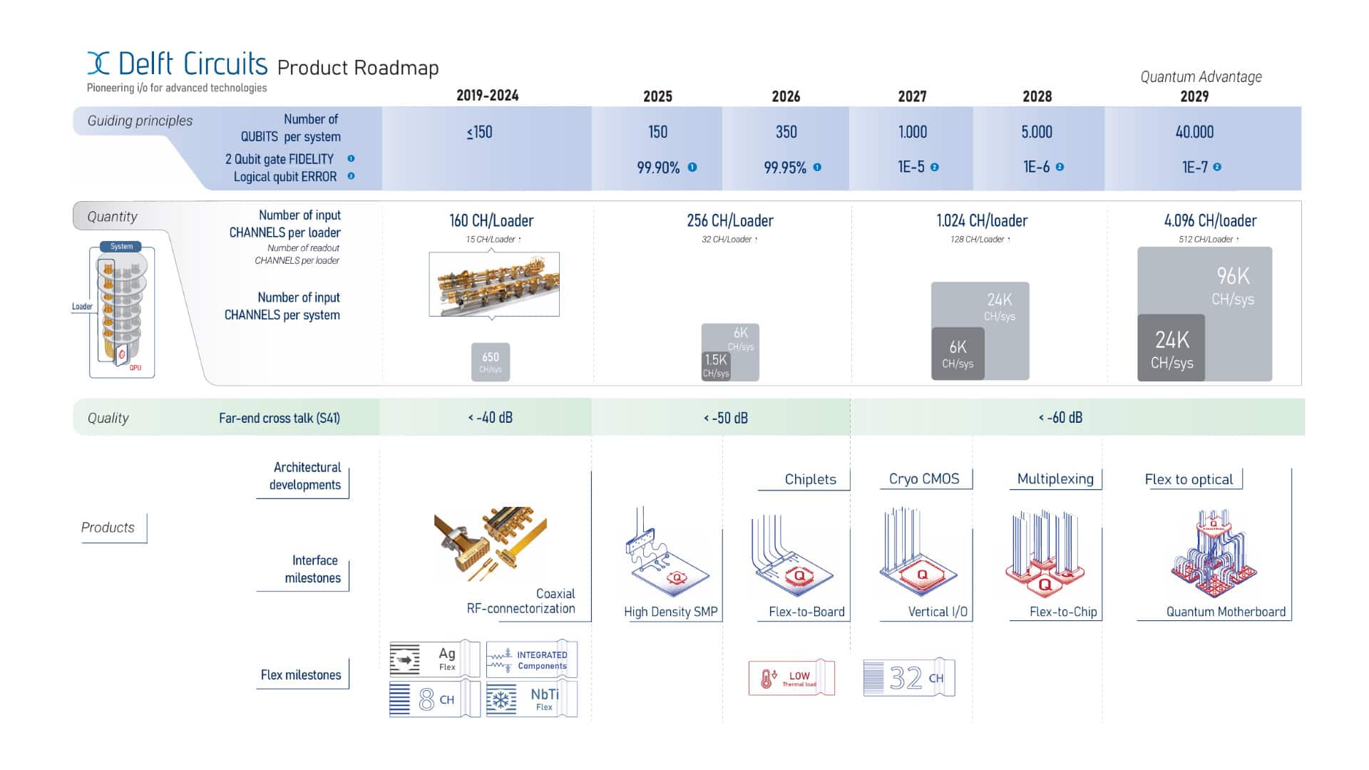
Quantum alignment The new product development roadmap from Delft Circuits starts with the guiding principles, highlighting performance milestones to be achieved by the quantum computing industry over the next five years – specifically, the number of physical qubits per system and gate fidelities. By extension, cabling metrics in the Delft Circuits roadmap focus on “quantity”: the number of I/O channels per loader (i.e. the wiring trees that insert into a cryostat, with typical cryostats having between 6–24 slots for loaders) and the number of channels per cryostat (summing across all loaders); also on “quality” (the crosstalk in the cabling flex). To complete the picture, the roadmap outlines product introductions at a conceptual level to enable both the quantity and quality timelines. (Courtesy: Delft Circuits)
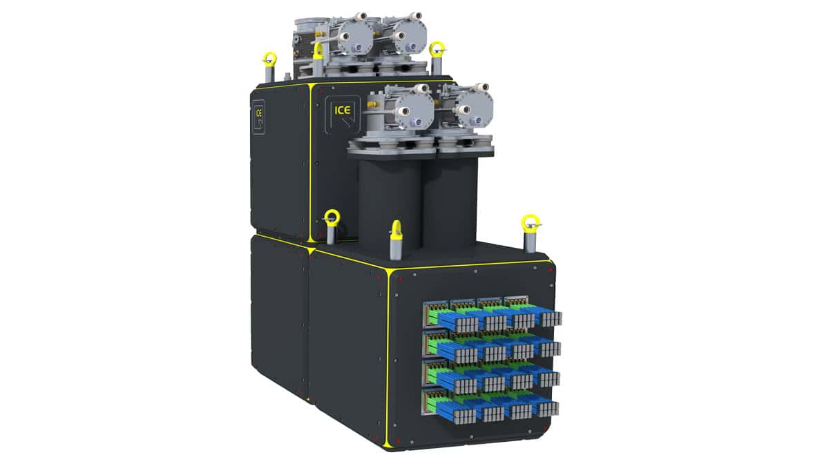
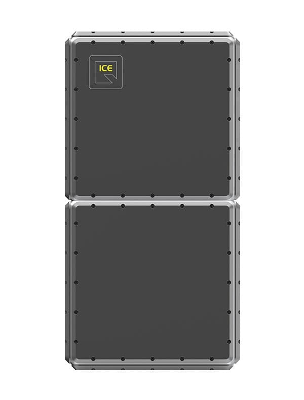
Modular and scalable: the ICE-Q cryogenics platform delivers the performance and reliability needed for professional computing environments while also providing a flexible and extendable design. The standard configuration includes a cooling module, a payload with a large sample space, and a side-loading wiring module for scalable connectivity (Courtesy: ICEoxford)
At the centre of most quantum labs is a large cylindrical cryostat that keeps the delicate quantum hardware at ultralow temperatures. These cryogenic chambers have expanded to accommodate larger and more complex quantum systems, but the scientists and engineers at UK-based cryogenics specialist ICEoxford have taken a radical new approach to the challenge of scalability. They have split the traditional cryostat into a series of cube-shaped modules that slot into a standard 19-inch rack mount, creating an adaptable platform that can easily be deployed alongside conventional computing infrastructure.
“We wanted to create a robust, modular and scalable solution that enables different quantum technologies to be integrated into the cryostat,” says Greg Graf, the company’s engineering manager. “This approach offers much more flexibility, because it allows different modules to be used for different applications, while the system also delivers the efficiency and reliability that are needed for operational use.”
The standard configuration of the ICE-Q platform has three separate modules: a cryogenics unit that provides the cooling power, a large payload for housing the quantum chip or experiment, and a patent-pending wiring module that attaches to the side of the payload to provide the connections to the outside world. Up to four of these side-loading wiring modules can be bolted onto the payload at the same time, providing thousands of external connections while still fitting into a standard rack. For applications where space is not such an issue, the payload can be further extended to accommodate larger quantum assemblies and potentially tens of thousands of radio-frequency or fibre-optic connections.
The cube-shaped form factor provides much improved access to these external connections, whether for designing and configuring the system or for ongoing maintenance work. The outer shell of each module consists of panels that are easily removed, offering a simple mechanism for bolting modules together or stacking them on top of each other to provide a fully scalable solution that grows with the qubit count.
The flexible design also offers a more practical solution for servicing or upgrading an installed system, since individual modules can be simply swapped over as and when needed. “For quantum computers running in an operational environment it is really important to minimize the downtime,” says Emma Yeatman, senior design engineer at ICEoxford. “With this design we can easily remove one of the modules for servicing, and replace it with another one to keep the system running for longer. For critical infrastructure devices, it is possible to have built-in redundancy that ensures uninterrupted operation in the event of a failure.”
Other features have been integrated into the platform to make it simple to operate, including a new software system for controlling and monitoring the ultracold environment. “Most of our cryostats have been designed for researchers who really want to get involved and adapt the system to meet their needs,” adds Yeatman. “This platform offers more options for people who want an out-of-the-box solution and who don’t want to get hands on with the cryogenics.”
Such a bold design choice was enabled in part by a collaborative research project with Canadian company Photonic Inc, funded jointly by the UK and Canada, that was focused on developing an efficient and reliable cryogenics platform for practical quantum computing. That R&D funding helped to reduce the risk of developing an entirely new technology platform that addresses many of the challenges that ICEoxford and its customers had experienced with traditional cryostats. “Quantum technologies typically need a lot of wiring, and access had become a real issue,” says Yeatman. “We knew there was an opportunity to do better.”
However, converting a large cylindrical cryostat into a slimline and modular form factor demanded some clever engineering solutions. Perhaps the most obvious was creating a frame that allows the modules to be bolted together while still remaining leak tight. Traditional cryostats are welded together to ensure a leak-proof seal, but for greater flexibility the ICEoxford team developed an assembly technique based on mechanical bonding.
The side-loading wiring module also presented a design challenge. To squeeze more wires into the available space, the team developed a high-density connector for the coaxial cables to plug into. An additional cold-head was also integrated into the module to pre-cool the cables, reducing the overall heat load generated by such large numbers of connections entering the ultracold environment.
Flexible for the future: the outer shell of the modules is covered with removable panels that make it easy to extend or reconfigure the system (Courtesy: ICEoxford)
Meanwhile, the speed of the cooldown and the efficiency of operation have been optimized by designing a new type of heat exchanger that is fabricated using a 3D printing process. “When warm gas is returned into the system, a certain amount of cooling power is needed just to compress and liquefy that gas,” explains Kelly. “We designed the heat exchangers to exploit the returning cold gas much more efficiently, which enables us to pre-cool the warm gas and use less energy for the liquefaction.”
The initial prototype has been designed to operate at 1 K, which is ideal for the photonics-based quantum systems being developed by ICEoxford’s research partner. But the modular nature of the platform allows it to be adapted to diverse applications, with a second project now underway with the Rutherford Appleton Lab to develop a module that that will be used at the forefront of the global hunt for dark matter.
Already on the development roadmap are modules that can sustain temperatures as low as 10 mK – which is typically needed for superconducting quantum computing – and a 4 K option for trapped-ion systems. “We already have products for each of those applications, but our aim was to create a modular platform that can be extended and developed to address the changing needs of quantum developers,” says Kelly.
As these different options come onstream, the ICEoxford team believes that it will become easier and quicker to deliver high-performance cryogenic systems that are tailored to the needs of each customer. “It normally takes between six and twelve months to build a complex cryogenics system,” says Graf. “With this modular design we will be able to keep some of the components on the shelf, which would allow us to reduce the lead time by several months.”
More generally, the modular and scalable platform could be a game-changer for commercial organizations that want to exploit quantum computing in their day-to-day operations, as well as for researchers who are pushing the boundaries of cryogenics design with increasingly demanding specifications. “This system introduces new avenues for hardware development that were previously constrained by the existing cryogenics infrastructure,” says Kelly. “The ICE-Q platform directly addresses the need for colder base temperatures, larger sample spaces, higher cooling powers, and increased connectivity, and ensures our clients can continue their aggressive scaling efforts without being bottlenecked by their cooling environment.”
You can find out more about the ICE-Q platform by contacting the ICEoxford team at iceoxford.com, or via email at sales@iceoxford.com. They will also be presenting the platform at the UK’s National Quantum Technologies Showcase in London on 7 November, with a further launch at the American Physical Society meeting in March 2026.
This talk shows how integrating p-type NiO to form NiO/Ga₂O₃ heterojunction rectifiers overcomes that barrier, enabling record-class breakdown and Ampere-class operation. It will cover device structure/process optimization, thermal stability to high temperatures, and radiation response – with direct ties to today’s priorities: EV fast charging, AI data‑center power systems, and aerospace/space‑qualified power electronics.
An interactive Q&A session follows the presentation.
Jian-Sian Li
Jian-Sian Li received the PhD in chemical engineering from the University of Florida in 2024, where his research focused on NiO/β-Ga₂O₃ heterojunction power rectifiers, includes device design, process optimization, fast switching, high-temperature stability, and radiation tolerance (γ, neutron, proton). His work includes extensive electrical characterization and microscopy/TCAD analysis supporting device physics and reliability in harsh environments. Previously, he completed his BS and MS at National Taiwan University (2015, 2018), with research spanning phoretic/electrokinetic colloids, polymers for OFETs/PSCs, and solid-state polymer electrolytes for Li-ion batteries. He has since transitioned to industry at Micron Technology.
Quantum connections Measurement scientists are seeking to understand and quantify the relative performance of quantum computers from different manufacturers as well as across the myriad platform technologies. (Courtesy: iStock/Bartlomiej Wroblewski)
From quantum utility today to quantum advantage tomorrow: incumbent technology companies – among them Google, Amazon, IBM and Microsoft – and a wave of ambitious start-ups are on a mission to transform quantum computing from applied research endeavour to mainstream commercial opportunity. The end-game: quantum computers that can be deployed at-scale to perform computations significantly faster than classical machines while addressing scientific, industrial and commercial problems beyond the reach of today’s high-performance computing systems.
Meanwhile, as technology translation gathers pace across the quantum supply chain, government laboratories and academic scientists must maintain their focus on the “hard yards” of precompetitive research. That means prioritizing foundational quantum hardware and software technologies, underpinned by theoretical understanding, experimental systems, device design and fabrication – and pushing out along all these R&D pathways simultaneously.
Bringing order to disorder
Equally important is the requirement to understand and quantify the relative performance of quantum computers from different manufacturers as well as across the myriad platform technologies – among them superconducting circuits, trapped ions, neutral atoms as well as photonic and semiconductor processors. A case study in this regard is a broad-scope UK research collaboration that, for the past four years, has been reviewing, collecting and organizing a holistic taxonomy of metrics and benchmarks to evaluate the performance of quantum computers against their classical counterparts as well as the relative performance of competing quantum platforms.
Funded by the National Quantum Computing Centre (NQCC), which is part of the UK National Quantum Technologies Programme (NQTP), and led by scientists at the National Physical Laboratory (NPL), the UK’s National Metrology Institute, the cross-disciplinary consortium has taken on an endeavour that is as sprawling as it is complex. The challenge lies in the diversity of quantum hardware platforms in the mix; also the emergence of two different approaches to quantum computing – one being a gate-based framework for universal quantum computation, the other an analogue approach tailored to outperforming classical computers on specific tasks.
“Given the ambition of this undertaking, we tapped into a deep pool of specialist domain knowledge and expertise provided by university colleagues at Edinburgh, Durham, Warwick and several other centres-of-excellence in quantum,” explains Ivan Rungger, a principal scientist at NPL, professor in computer science at Royal Holloway, University of London, and lead scientist on the quantum benchmarking project. That core group consulted widely within the research community and with quantum technology companies across the nascent supply chain. “The resulting study,” adds Rungger, “positions transparent and objective benchmarking as a critical enabler for trust, comparability and commercial adoption of quantum technologies, aligning closely with NPL’s mission in quantum metrology and standards.”
Not all metrics are equal – or mature
Made to measure NPL’s Institute for Quantum Standards and Technology (above) is the UK’s national metrology institute for quantum science. (Courtesy: NPL)
For context, a number of performance metrics used to benchmark classical computers can also be applied directly to quantum computers, such as the speed of operations, the number of processing units, as well as the probability of errors to occur in the computation. That only goes so far, though, with all manner of dedicated metrics emerging in the past decade to benchmark the performance of quantum computers – ranging from their individual hardware components to entire applications.
Complexity reigns, it seems, and navigating the extensive literature can prove overwhelming, while the levels of maturity for different metrics varies significantly. Objective comparisons aren’t straightforward either – not least because variations of the same metric are commonly deployed; also the data disclosed together with a reported metric value is often not sufficient to reproduce the results.
“Many of the approaches provide similar overall qualitative performance values,” Rungger notes, “but the divergence in the technical implementation makes quantitative comparisons difficult and, by extension, slows progress of the field towards quantum advantage.”
The task then is to rationalize the metrics used to evaluate the performance for a given quantum hardware platform to a minimal yet representative set agreed across manufacturers, algorithm developers and end-users. These benchmarks also need to follow some agreed common approaches to fairly and objectively evaluate quantum computers from different equipment vendors.
With these objectives in mind, Rungger and colleagues conducted a deep-dive review that has yielded a comprehensive collection of metrics and benchmarks to allow holistic comparisons of quantum computers, assessing the quality of hardware components all the way to system-level performance and application-level metrics.
Drill down further and there’s a consistent format for each metric that includes its definition, a description of the methodology, the main assumptions and limitations, and a linked open-source software package implementing the methodology. The software transparently demonstrates the methodology and can also be used in practical, reproducible evaluations of all metrics.
“As research on metrics and benchmarks progresses, our collection of metrics and the associated software for performance evaluation are expected to evolve,” says Rungger. “Ultimately, the repository we have put together will provide a ‘living’ online resource, updated at regular intervals to account for community-driven developments in the field.”
From benchmarking to standards
Innovation being what it is, those developments are well under way. For starters, the importance of objective and relevant performance benchmarks for quantum computers has led several international standards bodies to initiate work on specific areas that are ready for standardization – work that, in turn, will give manufacturers, end-users and investors an informed evaluation of the performance of a range of quantum computing components, subsystems and full-stack platforms.
What’s evident is that the UK’s voice on metrics and benchmarking is already informing the collective conversation around standards development. “The quantum computing community and international standardization bodies are adopting a number of concepts from our approach to benchmarking standards,” notes Deep Lall, a quantum scientist in Rungger’s team at NPL and lead author of the study. “I was invited to present our work to a number of international standardization meetings and scientific workshops, opening up widespread international engagement with our research and discussions with colleagues across the benchmarking community.”
He continues: “We want the UK effort on benchmarking and metrics to shape the broader international effort. The hope is that the collection of metrics we have pulled together, along with the associated open-source software provided to evaluate them, will guide the development of standardized benchmarks for quantum computers and speed up the progress of the field towards practical quantum advantage.”
That’s a view echoed – and amplified – by Cyrus Larijani, NPL’s head of quantum programme. “As we move into the next phase of NPL’s quantum strategy, the importance of evidence-based decision making becomes ever-more critical,” he concludes. “By grounding our strategic choices in robust measurement science and real-world data, we ensure that our innovations not only push the boundaries of quantum technology but also deliver meaningful impact across industry and society.”
Further reading
Deep Lall et al. 2025 A review and collection of metrics and benchmarks for quantum computers: definitions, methodologies and software https://arxiv.org/abs/2502.06717
The headline take from NQCC
Quantum computing technology has reached the stage where a number of methods for performance characterization are backed by a large body of real-world implementation and use, as well as by theoretical proofs. These mature benchmarking methods will benefit from commonly agreed-upon approaches that are the only way to fairly, unambiguously and objectively benchmark quantum computers from different manufacturers.
“Performance benchmarks are a fundamental enabler of technology innovation in quantum computing,” explains Konstantinos Georgopoulos, who heads up the NQCC’s quantum applications team and is responsible for the centre’s liaison with the NPL benchmarking consortium. “How do we understand performance? How do we compare capabilities? And, of course, what are the metrics that help us to do that? These are the leading questions we addressed through the course of this study.
”If the importance of benchmarking is a given, so too is collaboration and the need to bring research and industry stakeholders together from across the quantum ecosystem. “I think that’s what we achieved here,” says Georgopoulos. “The long list of institutions and experts who contributed their perspectives on quantum computing was crucial to the success of this project. What we’ve ended up with are better metrics, better benchmarks, and a better collective understanding to push forward with technology translation that aligns with end-user requirements across diverse industry settings.”
Professor Zhao Jiong, who leads a Master’s programme in microelectronics technology and material, has been recognized for his pioneering research in 2d ferroelectronics (Courtesy: PolyU)
The microelectronics sector is known for its relentless drive for innovation, continually delivering performance and efficiency gains within ever more compact form factors. Anyone aspiring to build a career in this fast-moving field needs not just a thorough grounding in current tools and techniques, but also an understanding of the next-generation materials and structures that will propel future progress.
That’s the premise behind a Master’s programme in microelectronics technology and materials at the Hong Kong Polytechnic University (PolyU). Delivered by the Department for Applied Physics, globally recognized for its pioneering research in technologies such as two-dimensional materials, nanoelectronics and artificial intelligence, the aim is to provide students with both the fundamental knowledge and practical skills they need to kickstart their professional future – whether they choose to pursue further research or to find a job in industry.
“The programme provides students with all the key skills they need to work in microelectronics, such as circuit design, materials processing and failure analysis,” says programme leader Professor Zhao Jiong, who research focuses on 2D ferroelectrics. “But they also have direct access to more than 20 faculty members who are actively investigating novel materials and structures that go beyond silicon-based technologies.”
The course in also unusual in providing a combined focus on electronics engineering and materials science, providing students with a thorough understanding of the underlying semiconductors and device structures as well as their use in mass-produced integrated circuits. That fundamental knowledge is reinforced through regular experimental work, providing the students with hands-on experience of fabricating and testing electronic devices. “Our cleanroom laboratory is equipped with many different instruments for microfabrication, including thin-film deposition, etching and photolithography, as well as advanced characterization tools for understanding their operating mechanisms and evaluating their performance,” adds Zhao.
In a module focusing on thin-film materials, for example, students gain valuable experience from practical sessions that enable them to operate the equipment for different growth techniques, such as sputtering, molecular beam epitaxy, and both physical and chemical vapour deposition. In another module on materials analysis and characterization, the students are tasked with analysing the layered structure of a standard computer chip by making cross-sections that can be studied with a scanning electron microscope.
During the programme students have access to a cleanroom laboratory that gives them hand-on experience of using advanced tools for fabricating and characterizing electronic materials and structures (Courtesy: PolyU)
That practical experience extends to circuit design, with students learning how to use state-of-the-art software tools for configuring, simulating and analysing complex electronic layouts. “Through this experimental work students gain the technical skills they need to design and fabricate integrated circuits, and to optimize their performance and reliability through techniques like failure analysis,” says Professor Dai Jiyan, PolyU Associate Dean of Students, who also teaches the module on thin-film materials. “This hands-on experience helps to prepare them for working in a manufacturing facility or for continuing their studies at the PhD level.”
Also integrated into the teaching programme is the use of artificial intelligence to assist key tasks, such as defect analysis, materials selection and image processing. Indeed, PolyU has established a joint laboratory with Huawei to investigate possible applications of AI tools in electronic design, providing the students with early exposure to emerging computational methods that are likely to shape the future of the microelectronics industry. “One of our key characteristics is that we embed AI into our teaching and laboratory work,” says Dai. “Two of the modules are directly related to AI, while the joint lab with Huawei helps students to experiment with using AI in circuit design.”
Now in its third year, the Master’s programme was designed in collaboration with Hong Kong’s Applied Science and Technology Research Institute (ASTRI), established in 2000 to enhance the competitiveness of the region through the use of advanced technologies. Researchers at PolyU already pursue joint projects with ASTRI in areas like chip design, microfabrication and failure analysis. As part of the programme, these collaborators are often invited to give guest lectures or to guide the laboratory work. “Sometimes they even provide some specialized instruments for the students to use in their experiments,” says Zhao. “We really benefit from this collaboration.”
Once primed with the knowledge and experience from the taught modules, the students have the opportunity to work alongside one of the faculty members on a short research project. They can choose whether to focus on a topic that is relevant to present-day manufacturing, such as materials processing or advanced packaging technologies, or to explore the potential of emerging materials and devices across applications ranging from solar cells and microfluidics to next-generation memories and neuromorphic computing.
“It’s very interesting for the students to get involved in these projects,” says Zhao. “They learn more about the research process, which can make them more confident to take their studies to the next level. All of our faculty members are engaged in important work, and we can guide the students towards a future research field if that’s what they are interested in.”
There are also plenty of progression opportunities for those who are more interested in pursuing a career in industry. As well as providing support and advice through its joint lab in AI, Huawei arranges visits to its manufacturing facilities and offers some internships to interested students. PolyU also organizes visits to Hong Kong’s Science Park, home to multinational companies such as Infineon as well as a large number of start-up companies in the microelectronics sector. Some of these might support a student’s research project, or offer an internship in areas such as circuit design or microfabrication.
The international outlook offered by PolyU has made the Master’s programme particularly appealing to students from mainland China, but Zhao and Dai believe that the forward-looking ethos of the course should make it an appealing option for graduates across Asia and beyond. “Through the programme, the students gain knowledge about all aspects of the microelectronics industry, and how it is likely to evolve in the future,” says Dai. “The knowledge and technical skills gained by the students offer them a competitive edge for building their future career, whether they want to find a job in industry or to continue their research studies.”