↩ Accueil

Vue lecture

Pioneers of 2D metals win the Physics World 2025 Breakthrough of the Year

Photograph of the apparatus used to create 2D metals
Under pressure A researcher in Beijing operates an apparatus used to make 2D metals. (Courtesy: CAS IOP/Handout via Xinhua)

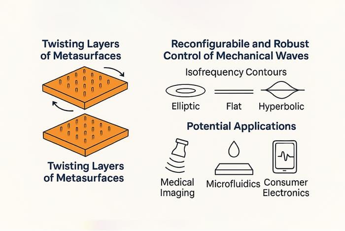
The Physics World 2025 Breakthrough of the Year is awarded to Guangyu ZhangLuojun Du  and colleagues at the Institute of Physics of the Chinese Academy of Sciences for producing the first 2D sheets of metal. The team produced five atomically thin 2D metals – bismuth, tin, lead, indium and gallium – with the thinnest being around 6.3 Å. The researchers say their work is just the “tip of the iceberg” and now aim to use their new materials to probe the fundamentals of physics. Their breakthrough could also lead to the development of new technologies.

Since the discovery of graphene – a sheet of carbon just one atom thick – in 2004, hundreds of other 2D materials have been fabricated and studied. In most of these, layers of covalently bonded atoms are separated by gaps where neighbouring layers are held together only by weak van der Waals (vdW) interactions, making it relatively easy to “shave off” single layers to make 2D sheets. Many thought that making atomically thin metals would be impossible given that each atom in a metal is strongly bonded to surrounding atoms in all directions.

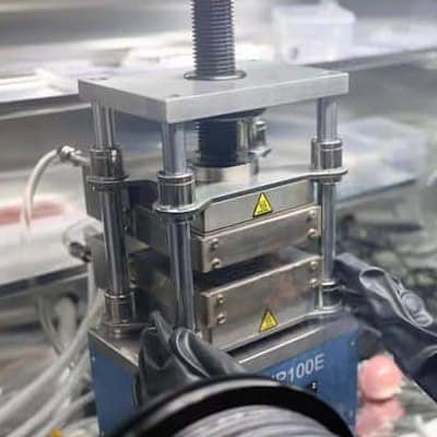
The technique developed by Zhang, Du and colleagues involves heating powders of pure metals between two monolayer-MoS2/sapphire vdW anvils. Once the metal powders are melted into a droplet, the researchers applied a pressure of 200 MPa and continued this “vdW squeezing” until the opposite sides of the anvils cooled to room temperature and 2D sheets of metal were formed.

“Right now, we have reported five single element metals, but actually we can do more because of the 88 metals in the periodic table,” Zhang explains in today’s episode of the Physics World Weekly podcast. In the podcast, he also talks about the team’s motivation creating 2D metals and some of the possible technological applications of the materials.

The Breakthrough of the Year was chosen by the Physics World editorial team. We looked back at all the scientific discoveries we have reported on since 1 January and picked the most important. In addition to being reported in Physics World in 2025, the breakthrough must meet the following criteria:

  • Significant advance in knowledge or understanding
  • Importance of work for scientific progress and/or development of real-world applications
  • Of general interest to Physics World readers

Before we picked our winners, we released the Physics World Top 10 Breakthroughs for 2025, which served as our shortlist. The other nine breakthroughs are listed below in no particular order.

Finding the stuff of life on an asteroid

Tim McCoy and Cari Corrigan
Analysing returned samples Tim McCoy (right), curator of meteorites at the Smithsonian’s National Museum of Natural History, and research geologist Cari Corrigan examine scanning electron microscope (SEM) images of a Bennu sample. (Courtesy: James Di Loreto, Smithsonian)

To Tim McCoy, Sara Russell, Danny Glavin, Jason Dworkin, Yoshihiro Furukawa, Ann Nguyen, Scott Sandford, Zack Gainsforth and an international team of collaborators for identifying salt, ammonia, sugar, nitrogen- and oxygen-rich organic materials, and traces of metal-rich supernova dust, in samples returned from the near-Earth asteroid 101955 Bennu. The incredible chemical richness of this asteroid, which NASA’s OSIRIS-REx spacecraft visited in 2020, lends support to the longstanding hypothesis that asteroid impacts could have “seeded” the early Earth with the raw ingredients needed for life to form. The discoveries also enhance our understanding of how Bennu and other objects in the solar system formed out of the disc of material that coalesced around the young Sun.

The first superfluid molecule

To Takamasa Momose of the University of British Columbia, Canada, and Susumu Kuma of the RIKEN Atomic, Molecular and Optical Physics Laboratory, Japan for observing superfluidity in a molecule for the first time. Molecular hydrogen is the simplest and lightest of all molecules, and theorists predicted that it would enter a superfluid state at a temperature between 1‒2 K. But this is well below the molecule’s freezing point of 13.8 K, so Momose, Kuma and colleagues first had to develop a way to keep the hydrogen in a liquid state. Once they did that, they then had to work out how to detect the onset of superfluidity. It took them nearly 20 years, but by confining clusters of hydrogen molecules inside helium nanodroplets, embedding a methane molecule within the clusters, and monitoring the methane’s rotation, they were finally able to do it. They now plan to study larger clusters of hydrogen, with the aim of exploring the boundary between classical and quantum behaviour in this system.

Hollow-core fibres break 40-year limit on light transmission

To researchers at the University of Southampton and Microsoft Azure Fiber in the UK, for developing a new type of optical fibre that reduces signal loss, boosts bandwidth and promises faster, greener communications. The team, led by Francesco Poletti, achieved this feat by replacing the glass core of a conventional fibre with air and using glass membranes that reflect light at certain frequencies back into the core to trap the light and keep it moving through the fibre’s hollow centre. Their results show that the hollow-core fibres exhibit 35% less attenuation than standard glass fibres – implying that fewer amplifiers would be needed in long cables – and increase transmission speeds by 45%. Microsoft has begun testing the new fibres in real systems, installing segments in its network and sending live traffic through them. These trials open the door to gradual rollout and Poletti suggests that the hollow-core fibres could one day replace existing undersea cables.

First patient treatments delivered with proton arc therapy

Trento Proton Therapy Centre researchers
PAT pioneers The research team in the proton therapy gantry room. (Courtesy: UO Fisica Sanitaria and UO Protonterapia, APSS, Trento)

To Francesco Fracchiolla and colleagues at the Trento Proton Therapy Centre in Italy for delivering the first clinical treatments using proton arc therapy (PAT). Proton therapy – a precision cancer treatment – is usually performed using pencil-beam scanning to precisely paint the dose onto the tumour. But this approach can be limited by the small number of beam directions deliverable in an acceptable treatment time. PAT overcomes this by moving to an arc trajectory with protons delivered over a large number of beam angles and the potential to optimize the number of energies used for each beam direction. Working with researchers at RaySearch Laboratories in Sweden, the team performed successful dosimetric comparisons with clinical proton therapy plans. Following a feasibility test that confirmed the viability of clinical PAT delivery, the researchers used PAT to treat nine cancer patients. Importantly, all treatments were performed using the centre’s existing proton therapy system and clinical workflow.

A protein qubit for quantum biosensing

To Peter Maurer and David Awschalom at the University of Chicago Pritzker School of Molecular Engineering and colleagues for designing a protein quantum bit (qubit) that can be produced directly inside living cells and used as a magnetic field sensor. While many of today’s quantum sensors are based on nitrogen–vacancy (NV) centres in diamond, they are large and hard to position inside living cells. Instead, the team used fluorescent proteins, which are just 3 nm in diameter and can be produced by cells at a desired location with atomic precision. These proteins possess similar optical and spin properties to those of NV centre-based qubits – namely that they have a metastable triplet state. The researchers used a near-infrared laser pulse to optically address a yellow fluorescent protein and read out its triplet spin state with up to 20% spin contrast. They then genetically modified the protein to be expressed in bacterial cells and measured signals with a contrast of up to 8%. They note that although this performance does not match that of NV quantum sensors, it could enable magnetic resonance measurements directly inside living cells, which NV centres cannot do.

Highest-resolution images ever taken of a single atom

To the team led by Yichao Zhang at the University of Maryland and Pinshane Huang of the University of Illinois at Urbana-Champaign for capturing the highest-resolution images ever taken of individual atoms in a material. The team used an electron-microscopy technique called electron ptychography to achieve a resolution of 15 pm, which is about 10 times smaller than the size of an atom. They studied a stack of two atomically-thin layers of tungsten diselenide, which were rotated relative to each other to create a moiré superlattice. These twisted 2D materials are of great interest to physicists because their electronic properties can change dramatically with small changes in rotation angle. The extraordinary resolution of their microscope allowed them to visualize collective vibrations in the material called moiré phasons. These are similar to phonons, but had never been observed directly until now. The team’s observations align with theoretical predictions for moiré phasons. Their microscopy technique should boost our understanding of the role that moiré phasons and other lattice vibrations play in the physics of solids. This could lead to the engineering of new and useful materials.

Quantum control of individual antiprotons

Photo of a physicist working at the BASE experiment
Exquisite control Physicist Barbara Latacz at the BASE experiment at CERN. (Courtesy: CERN)

To CERN’s BASE collaboration for being the first to perform coherent spin spectroscopy on a single antiproton – the antimatter counterpart of the proton. Their breakthrough is the most precise measurement yet of the antiproton’s magnetic properties, and could be used to test the Standard Model of particle physics. The experiment begins with the creation of high-energy antiprotons in an accelerator. These must be cooled (slowed down) to cryogenic temperatures without being lost to annihilation. Then, a single antiproton is held in an ultracold electromagnetic trap, where microwave pulses manipulate its spin state. The resulting resonance peak was 16 times narrower than previous measurements, enabling a significant leap in precision. This level of quantum control opens the door to highly sensitive comparisons of the properties of matter (protons) and antimatter (antiprotons). Unexpected differences could point to new physics beyond the Standard Model and may also reveal why there is much more matter than antimatter in the visible universe.

A smartphone-based early warning system for earthquakes

To Richard Allen, director of the Berkeley Seismological Laboratory at the University of California, Berkeley, and Google’s Marc Stogaitis and colleagues for creating a global network of Android smartphones that acts as an earthquake early warning system. Traditional early warning systems use networks of seismic sensors that rapidly detect earthquakes in areas close to the epicentre and issue warnings across the affected region. Building such seismic networks, however, is expensive, and many earthquake-prone regions do not have them. The researchers utilized the accelerometer in millions of phones in 98 countries to create the Android Earthquake Alert (AEA) system. Testing the app between 2021 and 2024 led to the detection of an average of 312 earthquakes a month, with magnitudes ranging from 1.9 to 7.8. For earthquakes of magnitude 4.5 or higher, the system sent “TakeAction” alerts to users, sending them, on average, 60 times per month for an average of 18 million individual alerts per month. The system also delivered lesser “BeAware” alerts to regions expected to experience a shaking intensity of magnitude 3 or 4. The team now aims to produce maps of ground shaking, which could assist the emergency response services following an earthquake.

A “weather map” for a gas giant exoplanet

To Lisa Nortmann at Germany’s University of Göttingen and colleagues for creating the first detailed “weather map” of an exoplanet. The forecast for exoplanet WASP-127b is brutal with winds reaching 33,000 km/hr, which is much faster than winds found anywhere in the Solar System. The WASP-127b is a gas giant located about 520 light–years from Earth and the team used the CRIRES+ instrument on the European Southern Observatory’s Very Large Telescope to observe the exoplanet as it transited across its star in less than 7 h. Spectral analysis of the starlight that filtered through WASP-127b’s atmosphere revealed Doppler shifts caused by supersonic equatorial winds. By analysing the range of Doppler shifts, the team created a rough weather map of  WASP-127b, even though they could not resolve light coming from specific locations on the exoplanet. Nortmann and colleagues concluded that the exoplanet’s poles are cooler that the rest of WASP-127b, where temperatures can exceed 1000 °C. Water vapour was detected in the atmosphere, raising the possibility of exotic forms of rain.

ROPP banner

Physics World‘s coverage of the Breakthrough of the Year is supported by Reports on Progress in Physics, which offers unparalleled visibility for your ground-breaking research.

The post Pioneers of 2D metals win the <em>Physics World</em> 2025 Breakthrough of the Year appeared first on Physics World.

  •  

How to make 2D metals: Guangyu Zhang on his team’s award-winning research

This episode of the Physics World Weekly podcast features Guangyu Zhang. Along with his colleagues at the Institute of Physics of the Chinese Academy of Sciences, Zhang has bagged the 2025 Physics World Breakthrough of the Year award for creating the first 2D metals.

In a wide-ranging conversation, we chat about the motivation behind the team’s research; the challenges in making 2D metals and how these were overcome; and how 2D metals could be used to boost our understanding of condensed matter physics and create new technologies.

I am also joined by my Physics World colleague Matin Durrani to talk about some of the exciting physics that we will be showcasing in 2025.

ROPP banner

Physics World‘s coverage of the Breakthrough of the Year is supported by Reports on Progress in Physics, which offers unparalleled visibility for your ground-breaking research.

The post How to make 2D metals: Guangyu Zhang on his team’s award-winning research appeared first on Physics World.

  •  

Slow spectroscopy sheds light on photodegradation

Using a novel spectroscopy technique, physicists in Japan have revealed how organic materials accumulate electrical charge through long-term illumination by sunlight – leading to material degradation. Ryota Kabe and colleagues at the Okinawa Institute of Science and Technology have shown how charge separation occurs gradually via a rare multi-photon ionization process, offering new insights into how plastics and organic semiconductors degrade in sunlight.

In a typical organic solar cell, an electron-donating material is interfaced with an electron acceptor. When the donor absorbs a photon, one of its electrons may jump across the interface, creating a bound electron-hole pair which may eventually dissociate – creating two free charges from which useful electrical work can be extracted.

Although such an interface vastly boosts the efficiency of this process, it is not necessary for charge separation to occur when an electron donor is illuminated. “Even single-component materials can generate tiny amounts of charge via multiphoton ionization,” Kabe explains. “However, experimental evidence has been scarce due to the extremely low probability of this process.”

To trigger charge separation in this way, an electron needs to absorb one or more additional photons while in its excited state. Since the vast majority of electrons fall back into their ground states before this can happen, the spectroscopic signature of this charge separation is very weak. This makes it incredibly difficult to detect using conventional spectroscopy techniques, which can generally only make observations over timescales of up to a few milliseconds.

The opposite approach

“While weak multiphoton pathways are easily buried under much stronger excited-state signals, we took the opposite approach in our work,” Kabe describes. “We excited samples for long durations and searched for traces of accumulated charges in the slow emission decay.”

Key to this approach was an electron donor called NPD. This organic material has a relatively long triplet lifetime, where an excited electron is prevented from transitioning back to its ground state. As a result, these molecules emit phosphorescence over relatively long timescales.

In addition, Kabe’s team dispersed their NPD samples into different host materials with carefully selected energy levels. In one medium, the energies of both the highest-occupied and lowest-unoccupied molecular orbitals lay below NPD’s corresponding levels, so that the host material acted as an electron acceptor. As a result, charge transfer occurred in the same way as it would across a typical donor-acceptor interface.

Yet in another medium, the host’s lowest-unoccupied orbital lay above NPD’s – blocking charge transfer, and allowing triplet states to accumulate instead. In this case, the only way for charge separation to occur was through multi-photon ionization.

Slow emission decay analysis

Since NPD’s long triplet lifetime allowed its electrons to be excited gradually over an extended period of illumination, its weak charge accumulation became detectable through slow emission decay analysis. In contrast, more conventional methods involve multiple, ultra-fast laser pulses, severely restricting the timescale over which measurements can be made. Altogether, this approach enabled the team to clearly distinguish between the two charge generation pathways.

“Using this method, we confirmed that charge generation occurred via resonance-enhanced multiphoton ionization mediated by long-lived triplet states, even in single-component organic materials,” Kabe describes.

This result offers insights into how plastics and organic semiconductors are degraded by sunlight over years or decades. The conventional explanation is that sunlight generates free radicals. These are molecules that lose an electron through ionization, leaving behind an unpaired electron which readily reacts with other molecules in the surrounding environment. Since photodegradation unfolds over such a long timescale, researchers could not observe this charge generation in single-component organic materials – until now.

“The method will be useful for analysing charge behaviour in organic semiconductor devices and for understanding long-term processes such as photodegradation that occur gradually under continuous light exposure,” Kabe says.

The research is described in Science Advances.

The post Slow spectroscopy sheds light on photodegradation appeared first on Physics World.

  •  

‘Patchy’ nanoparticles emerge from new atomic stencilling technique

Researchers in the US and Korea have created nanoparticles with carefully designed “patches” on their surfaces using a new atomic stencilling technique. These patches can be controlled with incredible precision, and could find use in targeted drug delivery, catalysis, microelectronics and tissue engineering.

The first step in the stencilling process is to create a mask on the surface of gold nanoparticles. This mask prevents a “paint” made from grafted-on polymers from attaching to certain areas of the nanoparticles.

“We then use iodide ions as a stencil,” explains Qian Chen, a materials scientist and engineer at the University of Illinois at Urbana-Champaign, US, who led the new research effort. “These adsorb (stick) to the surface of the nanoparticles in specific patterns that depend on the shape and atomic arrangement of the nanoparticles’ facets. That’s how we create the patches – the areas where the polymers selectively bind.” Chen adds that she and her collaborators can then tailor the surface chemistry of these tiny patchy nanoparticles in a very controlled way.

A gap in the field of microfabrication stencilling

The team decided to develop the technique after realizing there was a gap in the field of microfabrication stencilling. While techniques in this area have advanced considerably in recent years, allowing ever-smaller microdevices to be incorporated into ever-faster computer chips, most of them rely on top-down approaches for precisely controlling nanoparticles. By comparison, Chen says, bottom-up methods have been largely unexplored even though they are low-cost, solution-processable, scalable and compatible with complex, curved and three-dimensional surfaces.

Reporting their work in Nature, the researchers say they were inspired by the way proteins naturally self-assemble. “One of the holy grails in the field of nanomaterials is making complex, functional structures from nanoscale building blocks,” explains Chen. “It’s extremely difficult to control the direction and organization of each nanoparticle. Proteins have different surface domains, and thanks to their interactions with each other, they can make all the intricate machines we see in biology. We therefore adopted that strategy by creating patches or distinct domains on the surface of the nanoparticles.”

“Elegant and impressive”

Philip Moriarty, a physicist of the University of Nottingham, UK who was not involved in the project, describes it as “elegant and impressive” work. “Chen and colleagues have essentially introduced an entirely new mode of self-assembly that allows for much greater control of nanoparticle interactions,” he says, “and the ‘atomic stencil’ concept is clever and versatile.”

The team, which includes researchers at the University of Michigan, Pennsylvania State University, Cornell, Brookhaven National Laboratory and Korea’s Chonnam National University as well as Urbana-Champaign, agrees that the potential applications are vast. “Since we can now precisely control the surface properties of these nanoparticles, we can design them to interact with their environment in specific ways,” explains Chen. “That opens the door for more effective drug delivery, where nanoparticles can target specific cells. It could also lead to new types of catalysts, more efficient microelectronic components and even advanced materials with unique optical and mechanical properties.”

She and her colleagues say they now want to extend their approach to different types of nanoparticles and different substrates to find out how versatile it truly is. They will also be developing computational models that can predict the outcome of the stencilling process – something that would allow them to design and synthesize patchy nanoparticles for specific applications on demand.

The post ‘Patchy’ nanoparticles emerge from new atomic stencilling technique appeared first on Physics World.

  •  

New cylindrical metamaterials could act as shock absorbers for sensitive equipment

A 3D-printed structure called a kagome tube could form the backbone of a new system for muffling damaging vibrations. The structure is part of a class of materials known as topological mechanical metamaterials, and unlike previous materials in this group, it is simple enough to be deployed in real-world situations. According to lead developer James McInerney of the Wright-Patterson Air Force Base in Ohio, US, it could be used as shock protection for sensitive systems found in civil and aerospace engineering applications.

McInerney and colleagues’ tube-like design is made from a lattice of beams arranged in such a way that low-energy vibrational modes called floppy modes become localized to one side. “This provides good properties for isolating vibrations because energy input into the system on the floppy side does not propagate to the other side,” McInerney says.

The key to this desirable behaviour, he explains, is the arrangement of the beams that form the lattice structure. Using a pattern first proposed by the 19th century physicist James Clerk Maxwell, the beams are organized into repeating sub-units to form stable, two-dimensional structures known as topological Maxwell lattices.

Self-supporting design

Previous versions of these lattices could not support their own weight. Instead, they were attached to rigid external mounts, making it impractical to integrate them into devices. The new design, in contrast, is made by folding a flat Maxwell lattice into a cylindrical tube that is self-supporting. The tube features a connected inner and outer layer – a kagome bilayer – and its radius can be precisely engineered to give it the topological behaviour desired.

The researchers, who detail their work in Physical Review Applied, first tested their structure numerically by attaching a virtual version to a mechanically sensitive sample and a source of low-energy vibrations. As expected, the tube diverted the vibrations away from the sample and towards the other end of the tube.

Next, they developed a simple spring-and-mass model to understand the tube’s geometry by considering it as a simple monolayer. This modelling indicated that the polarization of the tube should be similar to the polarization of the monolayer. They then added rigid connectors to the tube’s ends and used a finite-element method to calculate the frequency-dependent patterns of vibrations propagating across the structure. They also determined the effective stiffness of the lattice as they applied loads parallel and perpendicular to it.

The researchers are targeting vibration-isolation applications that would benefit from a passive support structure, especially in cases where the performance of alternative passive mechanisms, such as viscoelastomers, is temperature-limited. “Our tubes do not necessarily need to replace other vibration isolation mechanisms,” McInerney explains. “Rather, they can enhance the capabilities of these by having the load-bearing structure assist with isolation.”

The team’s first and most important task, McInerney adds, will be to explore the implications of physically mounting the kagome tube on its vibration isolation structures. “The numerical study in our paper uses idealized mounting conditions so that the input and output are perfectly in phase with the tube vibrations,” he says. “Accounting for the potential impedance mismatch between the mounts and the tube will enable us to experimentally validate our work and provide realistic design scenarios.”

The post New cylindrical metamaterials could act as shock absorbers for sensitive equipment appeared first on Physics World.

  •  

Twistelastics controls how mechanical waves move in metamaterials

twisted surfaces can be used to manipulate mechanical waves
How it works Researchers use twisted surfaces to manipulate mechanical waves, enabling new technologies for imaging, electronics and sensors. (Courtesy: A Alù)

By simply placing two identical elastic metasurfaces atop each other and then rotating them relative to each other, the topology of the elastic waves dispersing through the resulting stacked structure can be changed – from elliptic to hyperbolic. This new control technique, from physicists at the CUNY Advanced Science Research Center in the US, works over a broad frequency range and has been dubbed “twistelastics”. It could allow for advanced reconfigurable phononic devices with potential applications in microelectronics, ultrasound sensing and microfluidics.

The researchers, led by Andrea Alù, say they were inspired by the recent advances in “twistronics” and its “profound impact” on electronic and photonic systems. “Our goal in this work was to explore whether similar twist-induced topological phenomena could be harnessed in elastodynamics in which phonons (vibrations of the crystal lattice) play a central role,” says Alù.

In twistelastics, the rotations between layers of identical, elastic engineered surfaces are used to manipulate how mechanical waves travel through the materials. The new approach, say the CUNY researchers, allows them to reconfigure the behaviour of these waves and precisely control them. “This opens the door to new technologies for sensing, communication and signal processing,” says Alù.

From elliptic to hyperbolic

In their work, the researchers used computer simulations to design metasurfaces patterned with micron-sized pillars. When they stacked one such metasurface atop the other and rotated them at different angles, the resulting combined structure changed the way phonons spread. Indeed, their dispersion topology went from elliptic to hyperbolic.

At a specific rotation angle, known as the “magic angle” (just like in twistronics), the waves become highly focused and begin to travel in one direction. This effect could allow for more efficient signal processing, says Alù, with the signals being easier to control over a wide range of frequencies.

The new twistelastic platform offers broadband, reconfigurable, and robust control over phonon propagation,” he tells Physics World. “This may be highly useful for a wide range of application areas, including surface acoustic wave (SAW) technologies, ultrasound imaging and sensing, microfluidic particle manipulation and on-chip phononic signal processing.

New frontiers

Since the twist-induced transitions are topologically protected, again like in twistronics, the system is resilient to fabrication imperfections, meaning it can be miniaturized and integrated into real-world devices, he adds. “We are part of an exciting science and technology centre called ‘New Frontiers of Sound’, of which I am one of the leaders. The goal of this ambitious centre is to develop new acoustic platforms for the above applications enabling disruptive advances for these technologies.”

Looking ahead, the researchers say they are looking into miniaturizing their metasurface design for integration into microelectromechanical systems (MEMS). They will also be studying multi-layer twistelastic architectures to improve how they can control wave propagation and investigating active tuning mechanisms, such as electromechanical actuation, to dynamically control twist angles. “Adding piezoelectric phenomena for further control and coupling to the electromagnetic waves,” is also on the agenda says Alù.

The present work is detailed in PNAS.

The post Twistelastics controls how mechanical waves move in metamaterials appeared first on Physics World.

  •  

Unlocking the potential of 2D materials: graphene and much more

This episode explores the scientific and technological significance of 2D materials such as graphene. My guest is Antonio Rossi, who is a researcher in 2D materials engineering at the Italian Institute of Technology in Genoa.

Rossi explains why 2D materials are fundamentally different than their 3D counterparts – and how these differences are driving scientific progress and the development of new and exciting technologies.

Graphene is the most famous 2D material and Rossi talks about today’s real-world applications of graphene in coatings. We also chat about the challenges facing scientists and engineers who are trying to exploit graphene’s unique electronic properties.

Rossi’s current research focuses on two other promising 2D materials – tungsten disulphide and hexagonal boron nitride. He explains why tungsten disulphide shows great technological promise because of its favourable electronic and optical properties; and why hexagonal boron nitride is emerging as an ideal substrate for creating 2D devices.

Artificial intelligence (AI) is becoming an important tool in developing new 2D materials. Rossi explains how his team is developing feedback loops that connect AI with the fabrication and characterization of new materials. Our conversation also touches on the use of 2D materials in quantum science and technology.

IOP Publishing’s new Progress In Series: Research Highlights website offers quick, accessible summaries of top papers from leading journals like Reports on Progress in Physics and Progress in Energy. Whether you’re short on time or just want the essentials, these highlights help you expand your knowledge of leading topics.

The post Unlocking the potential of 2D materials: graphene and much more appeared first on Physics World.

  •  
❌