↩ Accueil

Vue lecture

Modular cryogenics platform adapts to new era of practical quantum computing

2025-10-iceoxford-creo-main-image
Modular and scalable: the ICE-Q cryogenics platform delivers the performance and reliability needed for professional computing environments while also providing a flexible and extendable design. The standard configuration includes a cooling module, a payload with a large sample space, and a side-loading wiring module for scalable connectivity (Courtesy: ICEoxford)

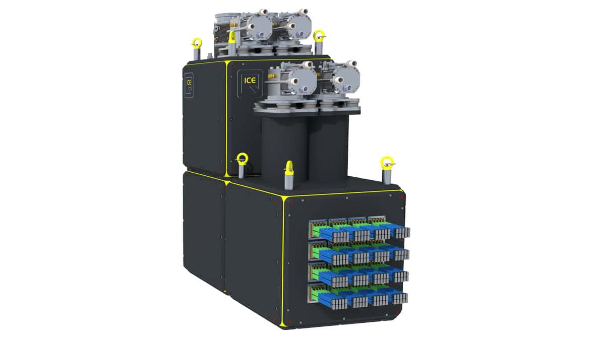
At the centre of most quantum labs is a large cylindrical cryostat that keeps the delicate quantum hardware at ultralow temperatures. These cryogenic chambers have expanded to accommodate larger and more complex quantum systems, but the scientists and engineers at UK-based cryogenics specialist ICEoxford have taken a radical new approach to the challenge of scalability. They have split the traditional cryostat into a series of cube-shaped modules that slot into a standard 19-inch rack mount, creating an adaptable platform that can easily be deployed alongside conventional computing infrastructure.

“We wanted to create a robust, modular and scalable solution that enables different quantum technologies to be integrated into the cryostat,” says Greg Graf, the company’s engineering manager. “This approach offers much more flexibility, because it allows different modules to be used for different applications, while the system also delivers the efficiency and reliability that are needed for operational use.”

The standard configuration of the ICE-Q platform has three separate modules: a cryogenics unit that provides the cooling power, a large payload for housing the quantum chip or experiment, and a patent-pending wiring module that attaches to the side of the payload to provide the connections to the outside world. Up to four of these side-loading wiring modules can be bolted onto the payload at the same time, providing thousands of external connections while still fitting into a standard rack. For applications where space is not such an issue, the payload can be further extended to accommodate larger quantum assemblies and potentially tens of thousands of radio-frequency or fibre-optic connections.

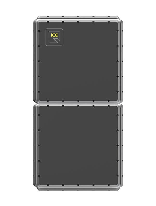
The cube-shaped form factor provides much improved access to these external connections, whether for designing and configuring the system or for ongoing maintenance work. The outer shell of each module consists of panels that are easily removed, offering a simple mechanism for bolting modules together or stacking them on top of each other to provide a fully scalable solution that grows with the qubit count.

The flexible design also offers a more practical solution for servicing or upgrading an installed system, since individual modules can be simply swapped over as and when needed. “For quantum computers running in an operational environment it is really important to minimize the downtime,” says Emma Yeatman, senior design engineer at ICEoxford. “With this design we can easily remove one of the modules for servicing, and replace it with another one to keep the system running for longer. For critical infrastructure devices, it is possible to have built-in redundancy that ensures uninterrupted operation in the event of a failure.”

Other features have been integrated into the platform to make it simple to operate, including a new software system for controlling and monitoring the ultracold environment. “Most of our cryostats have been designed for researchers who really want to get involved and adapt the system to meet their needs,” adds Yeatman. “This platform offers more options for people who want an out-of-the-box solution and who don’t want to get hands on with the cryogenics.”

Such a bold design choice was enabled in part by a collaborative research project with Canadian company Photonic Inc, funded jointly by the UK and Canada, that was focused on developing an efficient and reliable cryogenics platform for practical quantum computing. That R&D funding helped to reduce the risk of developing an entirely new technology platform that addresses many of the challenges that ICEoxford and its customers had experienced with traditional cryostats. “Quantum technologies typically need a lot of wiring, and access had become a real issue,” says Yeatman. “We knew there was an opportunity to do better.”

However, converting a large cylindrical cryostat into a slimline and modular form factor demanded some clever engineering solutions. Perhaps the most obvious was creating a frame that allows the modules to be bolted together while still remaining leak tight. Traditional cryostats are welded together to ensure a leak-proof seal, but for greater flexibility the ICEoxford team developed an assembly technique based on mechanical bonding.

The side-loading wiring module also presented a design challenge. To squeeze more wires into the available space, the team developed a high-density connector for the coaxial cables to plug into. An additional cold-head was also integrated into the module to pre-cool the cables, reducing the overall heat load generated by such large numbers of connections entering the ultracold environment.

2025-10-iceoxford-image-a4-system-render
Flexible for the future: the outer shell of the modules is covered with removable panels that make it easy to extend or reconfigure the system (Courtesy: ICEoxford)

Meanwhile, the speed of the cooldown and the efficiency of operation have been optimized by designing a new type of heat exchanger that is fabricated using a 3D printing process. “When warm gas is returned into the system, a certain amount of cooling power is needed just to compress and liquefy that gas,” explains Kelly. “We designed the heat exchangers to exploit the returning cold gas much more efficiently, which enables us to pre-cool the warm gas and use less energy for the liquefaction.”

The initial prototype has been designed to operate at 1 K, which is ideal for the photonics-based quantum systems being developed by ICEoxford’s research partner. But the modular nature of the platform allows it to be adapted to diverse applications, with a second project now underway with the Rutherford Appleton Lab to develop a module that that will be used at the forefront of the global hunt for dark matter.

Already on the development roadmap are modules that can sustain temperatures as low as 10 mK – which is typically needed for superconducting quantum computing – and a 4 K option for trapped-ion systems. “We already have products for each of those applications, but our aim was to create a modular platform that can be extended and developed to address the changing needs of quantum developers,” says Kelly.

As these different options come onstream, the ICEoxford team believes that it will become easier and quicker to deliver high-performance cryogenic systems that are tailored to the needs of each customer. “It normally takes between six and twelve months to build a complex cryogenics system,” says Graf. “With this modular design we will be able to keep some of the components on the shelf, which would allow us to reduce the lead time by several months.”

More generally, the modular and scalable platform could be a game-changer for commercial organizations that want to exploit quantum computing in their day-to-day operations, as well as for researchers who are pushing the boundaries of cryogenics design with increasingly demanding specifications. “This system introduces new avenues for hardware development that were previously constrained by the existing cryogenics infrastructure,” says Kelly. “The ICE-Q platform directly addresses the need for colder base temperatures, larger sample spaces, higher cooling powers, and increased connectivity, and ensures our clients can continue their aggressive scaling efforts without being bottlenecked by their cooling environment.”

  • You can find out more about the ICE-Q platform by contacting the ICEoxford team at iceoxford.com, or via email at sales@iceoxford.com. They will also be presenting the platform at the UK’s National Quantum Technologies Showcase in London on 7 November, with a further launch at the American Physical Society meeting in March 2026.

The post Modular cryogenics platform adapts to new era of practical quantum computing appeared first on Physics World.

  •  

Fabrication and device performance of Ni0/Ga2O3 heterojunction power rectifiers

ecs webinar image

This talk shows how integrating p-type NiO to form NiO/GaO heterojunction rectifiers overcomes that barrier, enabling record-class breakdown and Ampere-class operation. It will cover device structure/process optimization, thermal stability to high temperatures, and radiation response – with direct ties to today’s priorities: EV fast charging, AI data‑center power systems, and aerospace/space‑qualified power electronics.

An interactive Q&A session follows the presentation.


Jian-Sian Li

Jian-Sian Li received the PhD in chemical engineering from the University of Florida in 2024, where his research focused on NiO/β-GaO heterojunction power rectifiers, includes device design, process optimization, fast switching, high-temperature stability, and radiation tolerance (γ, neutron, proton). His work includes extensive electrical characterization and microscopy/TCAD analysis supporting device physics and reliability in harsh environments. Previously, he completed his BS and MS at National Taiwan University (2015, 2018), with research spanning phoretic/electrokinetic colloids, polymers for OFETs/PSCs, and solid-state polymer electrolytes for Li-ion batteries. He has since transitioned to industry at Micron Technology.

The post Fabrication and device performance of Ni0/Ga<sub>2</sub>O<sub>3</sub> heterojunction power rectifiers appeared first on Physics World.

  •  

Performance metrics and benchmarks point the way to practical quantum advantage

Quantum connections Measurement scientists are seeking to understand and quantify the relative performance of quantum computers from different manufacturers as well as across the myriad platform technologies. (Courtesy: iStock/Bartlomiej Wroblewski)

From quantum utility today to quantum advantage tomorrow: incumbent technology companies – among them Google, Amazon, IBM and Microsoft – and a wave of ambitious start-ups are on a mission to transform quantum computing from applied research endeavour to mainstream commercial opportunity. The end-game: quantum computers that can be deployed at-scale to perform computations significantly faster than classical machines while addressing scientific, industrial and commercial problems beyond the reach of today’s high-performance computing systems.

Meanwhile, as technology translation gathers pace across the quantum supply chain, government laboratories and academic scientists must maintain their focus on the “hard yards” of precompetitive research. That means prioritizing foundational quantum hardware and software technologies, underpinned by theoretical understanding, experimental systems, device design and fabrication – and pushing out along all these R&D pathways simultaneously.

Bringing order to disorder

Equally important is the requirement to understand and quantify the relative performance of quantum computers from different manufacturers as well as across the myriad platform technologies – among them superconducting circuits, trapped ions, neutral atoms as well as photonic and semiconductor processors. A case study in this regard is a broad-scope UK research collaboration that, for the past four years, has been reviewing, collecting and organizing a holistic taxonomy of metrics and benchmarks to evaluate the performance of quantum computers against their classical counterparts as well as the relative performance of competing quantum platforms.

Funded by the National Quantum Computing Centre (NQCC), which is part of the UK National Quantum Technologies Programme (NQTP), and led by scientists at the National Physical Laboratory (NPL), the UK’s National Metrology Institute, the cross-disciplinary consortium has taken on an endeavour that is as sprawling as it is complex. The challenge lies in the diversity of quantum hardware platforms in the mix; also the emergence of two different approaches to quantum computing – one being a gate-based framework for universal quantum computation, the other an analogue approach tailored to outperforming classical computers on specific tasks.

“Given the ambition of this undertaking, we tapped into a deep pool of specialist domain knowledge and expertise provided by university colleagues at Edinburgh, Durham, Warwick and several other centres-of-excellence in quantum,” explains Ivan Rungger, a principal scientist at NPL, professor in computer science at Royal Holloway, University of London, and lead scientist on the quantum benchmarking project. That core group consulted widely within the research community and with quantum technology companies across the nascent supply chain. “The resulting study,” adds Rungger, “positions transparent and objective benchmarking as a critical enabler for trust, comparability and commercial adoption of quantum technologies, aligning closely with NPL’s mission in quantum metrology and standards.”

Not all metrics are equal – or mature

2025-10-npl-na-aqml-image
Made to measure NPL’s Institute for Quantum Standards and Technology (above) is the UK’s national metrology institute for quantum science. (Courtesy: NPL)

For context, a number of performance metrics used to benchmark classical computers can also be applied directly to quantum computers, such as the speed of operations, the number of processing units, as well as the probability of errors to occur in the computation. That only goes so far, though, with all manner of dedicated metrics emerging in the past decade to benchmark the performance of quantum computers – ranging from their individual hardware components to entire applications.

Complexity reigns, it seems, and navigating the extensive literature can prove overwhelming, while the levels of maturity for different metrics varies significantly. Objective comparisons aren’t straightforward either – not least because variations of the same metric are commonly deployed; also the data disclosed together with a reported metric value is often not sufficient to reproduce the results.

“Many of the approaches provide similar overall qualitative performance values,” Rungger notes, “but the divergence in the technical implementation makes quantitative comparisons difficult and, by extension, slows progress of the field towards quantum advantage.”

The task then is to rationalize the metrics used to evaluate the performance for a given quantum hardware platform to a minimal yet representative set agreed across manufacturers, algorithm developers and end-users. These benchmarks also need to follow some agreed common approaches to fairly and objectively evaluate quantum computers from different equipment vendors.

With these objectives in mind, Rungger and colleagues conducted a deep-dive review that has yielded a comprehensive collection of metrics and benchmarks to allow holistic comparisons of quantum computers, assessing the quality of hardware components all the way to system-level performance and application-level metrics.

Drill down further and there’s a consistent format for each metric that includes its definition, a description of the methodology, the main assumptions and limitations, and a linked open-source software package implementing the methodology. The software transparently demonstrates the methodology and can also be used in practical, reproducible evaluations of all metrics.

“As research on metrics and benchmarks progresses, our collection of metrics and the associated software for performance evaluation are expected to evolve,” says Rungger. “Ultimately, the repository we have put together will provide a ‘living’ online resource, updated at regular intervals to account for community-driven developments in the field.”

From benchmarking to standards

Innovation being what it is, those developments are well under way. For starters, the importance of objective and relevant performance benchmarks for quantum computers has led several international standards bodies to initiate work on specific areas that are ready for standardization – work that, in turn, will give manufacturers, end-users and investors an informed evaluation of the performance of a range of quantum computing components, subsystems and full-stack platforms.

What’s evident is that the UK’s voice on metrics and benchmarking is already informing the collective conversation around standards development. “The quantum computing community and international standardization bodies are adopting a number of concepts from our approach to benchmarking standards,” notes Deep Lall, a quantum scientist in Rungger’s team at NPL and lead author of the study. “I was invited to present our work to a number of international standardization meetings and scientific workshops, opening up widespread international engagement with our research and discussions with colleagues across the benchmarking community.”

He continues: “We want the UK effort on benchmarking and metrics to shape the broader international effort. The hope is that the collection of metrics we have pulled together, along with the associated open-source software provided to evaluate them, will guide the development of standardized benchmarks for quantum computers and speed up the progress of the field towards practical quantum advantage.”

That’s a view echoed – and amplified – by Cyrus Larijani, NPL’s head of quantum programme. “As we move into the next phase of NPL’s quantum strategy, the importance of evidence-based decision making becomes ever-more critical,” he concludes. “By grounding our strategic choices in robust measurement science and real-world data, we ensure that our innovations not only push the boundaries of quantum technology but also deliver meaningful impact across industry and society.”

Further reading

Deep Lall et al. 2025 A  review and collection of metrics and benchmarks for quantum computers: definitions, methodologies and software https://arxiv.org/abs/2502.06717

The headline take from NQCC

Quantum computing technology has reached the stage where a number of methods for performance characterization are backed by a large body of real-world implementation and use, as well as by theoretical proofs. These mature benchmarking methods will benefit from commonly agreed-upon approaches that are the only way to fairly, unambiguously and objectively benchmark quantum computers from different manufacturers.

“Performance benchmarks are a fundamental enabler of technology innovation in quantum computing,” explains Konstantinos Georgopoulos, who heads up the NQCC’s quantum applications team and is responsible for the centre’s liaison with the NPL benchmarking consortium. “How do we understand performance? How do we compare capabilities? And, of course, what are the metrics that help us to do that? These are the leading questions we addressed through the course of this study.

”If the importance of benchmarking is a given, so too is collaboration and the need to bring research and industry stakeholders together from across the quantum ecosystem. “I think that’s what we achieved here,” says Georgopoulos. “The long list of institutions and experts who contributed their perspectives on quantum computing was crucial to the success of this project. What we’ve ended up with are better metrics, better benchmarks, and a better collective understanding to push forward with technology translation that aligns with end-user requirements across diverse industry settings.”

End note: NPL retains copyright on this article.

The post Performance metrics and benchmarks point the way to practical quantum advantage appeared first on Physics World.

  •  

Master’s programme takes microelectronics in new directions

hong-kong-university-na-main-image
Professor Zhao Jiong, who leads a Master’s programme in microelectronics technology and material, has been recognized for his pioneering research in 2d ferroelectronics (Courtesy: PolyU)

The microelectronics sector is known for its relentless drive for innovation, continually delivering performance and efficiency gains within ever more compact form factors. Anyone aspiring to build a career in this fast-moving field needs not just a thorough grounding in current tools and techniques, but also an understanding of the next-generation materials and structures that will propel future progress.

That’s the premise behind a Master’s programme in microelectronics technology and materials at the Hong Kong Polytechnic University (PolyU). Delivered by the Department for Applied Physics, globally recognized for its pioneering research in technologies such as two-dimensional materials, nanoelectronics and artificial intelligence, the aim is to provide students with both the fundamental knowledge and practical skills they need to kickstart their professional future – whether they choose to pursue further research or to find a job in industry.

“The programme provides students with all the key skills they need to work in microelectronics, such as circuit design, materials processing and failure analysis,” says programme leader Professor Zhao Jiong, who research focuses on 2D ferroelectrics. “But they also have direct access to more than 20 faculty members who are actively investigating novel materials and structures that go beyond silicon-based technologies.”

The course in also unusual in providing a combined focus on electronics engineering and materials science, providing students with a thorough understanding of the underlying semiconductors and device structures as well as their use in mass-produced integrated circuits. That fundamental knowledge is reinforced through regular experimental work, providing the students with hands-on experience of fabricating and testing electronic devices. “Our cleanroom laboratory is equipped with many different instruments for microfabrication, including thin-film deposition, etching and photolithography, as well as advanced characterization tools for understanding their operating mechanisms and evaluating their performance,” adds Zhao.

In a module focusing on thin-film materials, for example, students gain valuable experience from practical sessions that enable them to operate the equipment for different growth techniques, such as sputtering, molecular beam epitaxy, and both physical and chemical vapour deposition. In another module on materials analysis and characterization, the students are tasked with analysing the layered structure of a standard computer chip by making cross-sections that can be studied with a scanning electron microscope.

During the programme students have access to a cleanroom laboratory that gives them hand-on experience of using advanced tools for fabricating and characterizing electronic materials and structures (Courtesy: PolyU)

That practical experience extends to circuit design, with students learning how to use state-of-the-art software tools for configuring, simulating and analysing complex electronic layouts. “Through this experimental work students gain the technical skills they need to design and fabricate integrated circuits, and to optimize their performance and reliability through techniques like failure analysis,” says Professor Dai Jiyan, PolyU Associate Dean of Students, who also teaches the module on thin-film materials. “This hands-on experience helps to prepare them for working in a manufacturing facility or for continuing their studies at the PhD level.”

Also integrated into the teaching programme is the use of artificial intelligence to assist key tasks, such as defect analysis, materials selection and image processing. Indeed, PolyU has established a joint laboratory with Huawei to investigate possible applications of AI tools in electronic design, providing the students with early exposure to emerging computational methods that are likely to shape the future of the microelectronics industry. “One of our key characteristics is that we embed AI into our teaching and laboratory work,” says Dai. “Two of the modules are directly related to AI, while the joint lab with Huawei helps students to experiment with using AI in circuit design.”

Now in its third year, the Master’s programme was designed in collaboration with Hong Kong’s Applied Science and Technology Research Institute (ASTRI), established in 2000 to enhance the competitiveness of the region through the use of advanced technologies. Researchers at PolyU already pursue joint projects with ASTRI in areas like chip design, microfabrication and failure analysis. As part of the programme, these collaborators are often invited to give guest lectures or to guide the laboratory work. “Sometimes they even provide some specialized instruments for the students to use in their experiments,” says Zhao. “We really benefit from this collaboration.”

Once primed with the knowledge and experience from the taught modules, the students have the opportunity to work alongside one of the faculty members on a short research project. They can choose whether to focus on a topic that is relevant to present-day manufacturing, such as materials processing or advanced packaging technologies, or to explore the potential of emerging materials and devices across applications ranging from solar cells and microfluidics to next-generation memories and neuromorphic computing.

“It’s very interesting for the students to get involved in these projects,” says Zhao. “They learn more about the research process, which can make them more confident to take their studies to the next level. All of our faculty members are engaged in important work, and we can guide the students towards a future research field if that’s what they are interested in.”

There are also plenty of progression opportunities for those who are more interested in pursuing a career in industry. As well as providing support and advice through its joint lab in AI, Huawei arranges visits to its manufacturing facilities and offers some internships to interested students. PolyU also organizes visits to Hong Kong’s Science Park, home to multinational companies such as Infineon as well as a large number of start-up companies in the microelectronics sector. Some of these might support a student’s research project, or offer an internship in areas such as circuit design or microfabrication.

The international outlook offered by PolyU has made the Master’s programme particularly appealing to students from mainland China, but Zhao and Dai believe that the forward-looking ethos of the course should make it an appealing option for graduates across Asia and beyond. “Through the programme, the students gain knowledge about all aspects of the microelectronics industry, and how it is likely to evolve in the future,” says Dai. “The knowledge and technical skills gained by the students offer them a competitive edge for building their future career, whether they want to find a job in industry or to continue their research studies.”

The post Master’s programme takes microelectronics in new directions appeared first on Physics World.

  •  
❌