↩ Accueil

Vue lecture

Staying the course with lockdowns could end future pandemics in months

As a theoretical and mathematical physicist at Imperial College London, UK, Bhavin Khatri spent years using statistical physics to understand how organisms evolve. Then the COVID-19 pandemic struck, and like many other scientists, he began searching for ways to apply his skills to the crisis. This led him to realize that the equations he was using to study evolution could be repurposed to model the spread of the virus – and, crucially, to understand how it could be curtailed.

In a paper published in EPL, Khatri models the spread of a SARS-CoV-2-like virus using branching process theory, which he’d previously used to study how advantageous alleles (variations in a genetic sequence) become more prevalent in a population. He then uses this model to assess the duration that interventions such as lockdowns would need to be applied in order to completely eliminate infections, with the strength of the intervention measured in terms of the number of people each infected person goes on to infect (the virus’ effective reproduction number, R).

Tantalizingly, the paper concludes that applying such interventions worldwide in June 2020 could have eliminated the COVID virus by January 2021, several months before the widespread availability of vaccines reduced its impact on healthcare systems and led governments to lift restrictions on social contact. Physics World spoke to Khatri to learn more about his research and its implications for future pandemics.

What are the most important findings in your work?

One important finding is that we can accurately calculate the distribution of times required for a virus to become extinct by making a relatively simple approximation. This approximation amounts to assuming that people have relatively little population-level “herd” immunity to the virus – exactly the situation that many countries, including the UK, faced in March 2020.

Making this approximation meant I could reduce the three coupled differential equations of the well-known SIR model (which models pandemics via the interplay between Susceptible, Infected and Recovered individuals) to a single differential equation for the number of infected individuals in the population. This single equation turned out to be the same one that physics students learn when studying radioactive decay. I then used the discrete stochastic version of exponential decay and standard approaches in branching process theory to calculate the distribution of extinction times.

Simulation trajectories a) A plot of the decline in the number of infected individuals over time. b) Probability density of extinction times for the same parameters as in a), showing that the most likely extinction times are measured in months. (Courtesy: Bhavin S. Khatri 2025 EPL 152 11003 DOI 10.1209/0295-5075/ae0c31 CC-BY 4.0 https://creativecommons.org/licenses/by/4.0/)

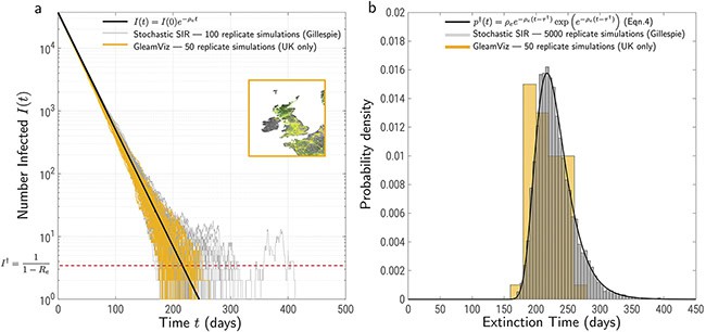
Alongside the formal theory, I also used my experience in population genetic theory to develop an intuitive approach for calculating the mean of this extinction time distribution. In population genetics, when a mutation is sufficiently rare, changes in its number of copies in the population are dominated by randomness. This is true even if the mutation has a large selective advantage: it has to grow by chance to sufficient critical size – on the order of 1/(selection strength) – for selection to take hold.

The same logic works in reverse when applied to a declining number of infections. Initially, they will decline deterministically, but once they go below a threshold number of individuals, changes in infection numbers become random. Using the properties of such random walks, I calculated an expression for the threshold number and the mean duration of the stochastic phase. These agree well with the formal branching process calculation.

In practical terms, the main result of this theoretical work is to show that for sufficiently strong lockdowns (where, on average, only one of every two infected individuals goes on to infect another person, R=0.5), this distribution of extinction times was narrow enough to ensure that the COVID pandemic virus would have gone extinct in a matter of months, or at most a year.

How realistic is this counterfactual scenario of eliminating SARS-CoV-2 within a year?

Leaving politics and the likelihood of social acceptance aside for the moment, if a sufficiently strong lockdown could have been maintained for a period of roughly six months across the globe, then I am confident that the virus could have been reduced to very low levels, or even made extinct.

The question then is: is this a stable situation? From the perspective of a single nation, if the rest of the world still has infections, then that nation either needs to maintain its lockdown or be prepared to re-impose it if there are new imported cases. From a global perspective, a COVID-free world should be a stable state, unless an animal reservoir of infections causes re-infections in humans.

Photo of Bhavin Khatri. He has a salt-and-pepper beard and glasses, he's wearing a button-down shirt with fine red checks that's open at the collar, and he's sitting in front of a window in an office
Modelling the decline of a virus: Theoretical physicist and biologist Bhavin Khatri. (Courtesy: Bhavin Khatri)

As for the practical success of such a strategy, that depends on politics and the willingness of individuals to remain in lockdown. Clearly, this is not in the model. One thing I do discuss, though, is that this strategy becomes far more difficult once more infectious variants of SARS-CoV-2 evolve. However, the problem I was working on before this one (which I eventually published in PNAS) concerned the probability of evolutionary rescue or resistance, and that work suggests that evolution of new COVID variants reduces significantly when there are fewer infections. So an elimination strategy should also be more robust against the evolution of new variants.

What lessons would you like experts (and the public) to take from this work when considering future pandemic scenarios?

I’d like them to conclude that pandemics with similar properties are, in principle, controllable to small levels of infection – or complete extinction – on timescales of months, not years, and that controlling them minimizes the chance of new variants evolving. So, although the question of the political and social will to enact such an elimination strategy is not in the scope of the paper, I think if epidemiologists, policy experts, politicians and the public understood that lockdowns have a finite time horizon, then it is more likely that this strategy could be adopted in the future.

I should also say that my work makes no comment on the social harms of lockdowns, which shouldn’t be minimized and would need to be weighed against the potential benefits.

What do you plan to do next?

I think the most interesting next avenue will be to develop theory that lets us better understand the stability of the extinct state at the national and global level, under various assumptions about declining infections in other countries that adopted different strategies and the role of an animal reservoir.

It would also be interesting to explore the role of “superspreaders”, or infected individuals who infect many other people. There’s evidence that many infections spread primarily through relatively few superspreaders, and heuristic arguments suggest that taking this into account would decrease the time to extinction compared to the estimates in this paper.

I’ve also had a long-term interest in understanding the evolution of viruses from the lens of what are known as genotype phenotype maps, where we consider the non-trivial and often redundant mapping from genetic sequences to function, where the role of stochasticity in evolution can be described by statistical physics analogies. For the evolution of the antibodies that help us avoid virus antigens, this would be a driven system, and theories of non-equilibrium statistical physics could play a role in answering questions about the evolution of new variants.

The post Staying the course with lockdowns could end future pandemics in months appeared first on Physics World.

  •  

Reversible degradation phenomenon in PEMWE cells


In proton exchange membrane water electrolysis (PEMWE) systems, voltage cycles dropping below a threshold are associated with reversible performance improvements, which remain poorly understood despite being documented in literature. The distinction between reversible and irreversible performance changes is crucial for accurate degradation assessments. One approach in literature to explain this behaviour is the oxidation and reduction of iridium. Iridium-based electrocatalyst activity and stability in PEMWE hinge on their oxidation state, influenced by the applied voltage. Yet, full-cell PEMWE dynamic performance remains under-explored, with a focus typically on stability rather than activity. This study systematically investigates reversible performance behaviour in PEMWE cells using Ir-black as an anodic catalyst. Results reveal a recovery effect when the low voltage level drops below 1.5 V, with further enhancements observed as the voltage decreases, even with a short holding time of 0.1 s. This reversible recovery is primarily driven by improved anode reaction kinetics, likely due to changing iridium oxidation states, and is supported by alignment between the experimental data and a dynamic model that links iridium oxidation/reduction processes to performance metrics. This model allows distinguishing between reversible and irreversible effects and enables the derivation of optimized operation schemes utilizing the recovery effect.

Tobias Krenz
Tobias Krenz

Tobias Krenz is a simulation and modelling engineer at Siemens Energy in the Transformation of Industry business area focusing on reducing energy consumption and carbon-dioxide emissions in industrial processes. He completed his PhD from Liebniz University Hannover in February 2025. He earned a degree from Berlin University of Applied Sciences in 2017 and a MSc from Technische Universität Darmstadt in 2020.

Alexander Rex
Alexander Rex


Alexander Rex is a PhD candidate at the Institute of Electric Power Systems at Leibniz University Hannover. He holds a degree in mechanical engineering from Technische Universität Braunschweig, an MEng from Tongji University, and an MSc from Karlsruhe Institute of Technology (KIT). He was a visiting scholar at Berkeley Lab from 2024 to 2025.

The post Reversible degradation phenomenon in PEMWE cells appeared first on Physics World.

  •  

Why quantum metrology is the driving force for best practice in quantum standardization

3d render quantum computer featuring qubit chip
Quantum advantage international standardization efforts will, over time, drive economies of scale and multivendor interoperability across the nascent quantum supply chain. (Courtesy: iStock/Peter Hansen)

How do standards support the translation of quantum science into at-scale commercial opportunities?

The standardization process helps to promote the legitimacy of emerging quantum technologies by distilling technical inputs and requirements from all relevant stakeholders across industry, research and government. Put simply: if you understand a technology well enough to standardize elements of it, that’s when you know it’s moved beyond hype and theory into something of practical use for the economy and society.

What are the upsides of standardization for developers of quantum technologies and, ultimately, for end-users in industry and the public sector?

Standards will, over time, help the quantum technology industry achieve critical mass on the supply side, with those economies of scale driving down prices and increasing demand. As the nascent quantum supply chain evolves – linking component manufacturers, subsystem developers and full-stack quantum computing companies – standards will also ensure interoperability between products from different vendors and different regions.

Those benefits flow downstream as well because standards, when implemented properly, increase trust among end-users by defining a minimum quality of products, processes and services. Equally important, as new innovations are rolled out into the marketplace by manufacturers, standards will ensure compatibility across current and next-generation quantum systems, reducing the likelihood of lock-ins to legacy technologies.

What’s your role in coordinating NPL’s standards effort in quantum science and technology?

I have strategic oversight of our core technical programmes in quantum computing, quantum networking, quantum metrology and quantum-enabled PNT (position, navigation and timing). It’s a broad-scope remit that spans research, training as well as responsibility for standardization and international collaboration, with the latter often going hand-in-hand.

Right now, we have over 150 people working within the NPL quantum metrology programme. Their collective focus is on developing the measurement science necessary to build, test and evaluate a wide range of quantum devices and systems. Our research helps innovators, whether in an industry or university setting, to push the limits of quantum technology by providing leading-edge capabilities and benchmarking to measure the performance of new quantum products and services.

Tim Prior
Tim Prior “We believe that quantum metrology and standardization are key enablers of quantum innovation.” (Courtesy: NPL)

It sounds like there are multiple layers of activity.

That’s right. For starters, we have a team focusing on the inter-country strategic relationships, collaborating closely with colleagues at other National Metrology Institutes (like NIST in the US and PTB in Germany). A key role in this regard is our standards specialist who, given his background working in the standards development organizations (SDOs), acts as a “connector” between NPL’s quantum metrology teams and, more widely, the UK’s National Quantum Technology Programme and the international SDOs.

We also have a team of technical experts who sit on specialist working groups within the SDOs. Their inputs to standards development are not about NPL’s interests, rather providing expertise and experience gained from cutting-edge metrology; also building a consolidated set of requirements gathered from stakeholders across the quantum community to further the UK’s strategic and technical priorities in quantum.

So NPL’s quantum metrology programme provides a focal point for quantum standardization?

Absolutely. We believe that quantum metrology and standardization are key enablers of quantum innovation, fast-tracking the adoption and commercialization of quantum technologies while building confidence among investors and across the quantum supply chain and early-stage user base. For NPL and its peers, the task right now is to agree on the terminology and best practice as we figure out the performance metrics, benchmarks and standards that will enable quantum to go mainstream.

How does NPL engage the UK quantum community on standards development?

Front-and-centre is the UK Quantum Standards Network Pilot. This initiative – which is being led by NPL – brings together representatives from industry, academia and government to work on all aspects of standards development: commenting on proposals and draft standards; discussing UK standards policy and strategy; and representing the UK in the European and international SDOs. The end-game? To establish the UK as a leading voice in quantum standardization, both strategically and technically, and to ensure that UK quantum technology companies have access to global supply chains and markets.

What about NPL outreach to prospective end-users of quantum technologies?

The Quantum Standards Network Pilot also provides a direct line to prospective end-users of quantum technologies in business sectors like finance, healthcare, pharmaceuticals and energy. What’s notable is that the end-users are often preoccupied with questions that link in one way or another to standardization. For example: how well do quantum technologies stack up against current solutions? Are quantum systems reliable enough yet? What does quantum cost to implement and maintain, including long-term operational costs? Are there other emerging technologies that could do the same job? Is there a solid, trustworthy supply chain?

It’s clear that international collaboration is mandatory for successful standards development. What are the drivers behind the recently announced NMI-Q collaboration?

The quantum landscape is changing fast, with huge scope for disruptive innovation in quantum computing, quantum communications and quantum sensing. Faced with this level of complexity, NMI-Q leverages the combined expertise of the world’s leading National Metrology Institutes – from the G7 countries and Australia – to accelerate the development and adoption of quantum technologies.

No one country can do it all when it comes to performance metrics, benchmarks and standards in quantum science and technology. As such, NMI-Q’s priorities are to conduct collaborative pre-standardization research; develop a set of “best measurement practices” needed by industry to fast-track quantum innovation; and, ultimately, shape the global standardization effort in quantum. NPL’s prominent role within NMI-Q (I am the co-chair along with Barbara Goldstein of NIST) underscores our commitment to evidence-based decision-making in standards development and, ultimately, to the creation of a thriving quantum ecosystem.

What are the attractions of NPL’s quantum programme for early-career physicists?

Every day, our measurement scientists address cutting-edge problems in quantum – as challenging as anything they’ll have encountered previously in an academic setting. What’s especially motivating, however, is that the NPL is a mission-driven endeavour with measurement outcomes linking directly to wider societal and economic benefits – not just in the UK, but internationally as well.

Quantum metrology: at your service

Measurement for Quantum (M4Q) is a flagship NPL programme that provides industry partners with up to 20 days of quantum metrology expertise to address measurement challenges in applied R&D and product development. The service – which is free of charge for projects approved after peer review – helps companies to bridge the gap from technology prototype to full commercialization.

To date, more than two-thirds of the companies to participate in M4Q report that their commercial opportunity has increased as a direct result of NPL support. In terms of specifics, the M4Q offering includes the following services:

  • Small-current and quantum-noise measurements
  • Measurement of material-induced noise in superconducting quantum circuits
  • Nanoscale imaging of physical properties for applications in quantum devices
  • Characterization of single-photon sources and detectors
  • Characterization of compact lasers and other photonic components
  • Semiconductor device characterisation at cryogenic temperatures

Apply for M4Q support here.

Further reading

Performance metrics and benchmarks point the way to practical quantum advantage

End note: NPL retains copyright on this article.

The post Why quantum metrology is the driving force for best practice in quantum standardization appeared first on Physics World.

  •  

SEMICON Europa 2025 presents cutting-edge technology for semiconductor R&D and production

“Global collaborations for European economic resilience” is the theme of  SEMICON Europa 2025. The event is coming to Munich, Germany on 18–21 November and it will attract 25,000 semiconductor professionals who will enjoy presentations from over 200 speakers.

The TechARENA portion of the event will cover a wide range of technology-related issues including new materials, future computing paradigms and the development of hi-tech skills in the European workface. There will also be an Executive Forum, which will feature leaders in industry and government and will cover topics including silicon geopolitics and the use of artificial intelligence in semiconductor manufacturing.

SEMICON Europa will be held at the Messe München, where it will feature a huge exhibition with over 500 exhibitors from around the world. The exhibition is spread out over three halls and here are some of the companies and product innovations to look out for on the show floor.

Accelerating the future of electro-photonic integration with SmarAct

As the boundaries between electronic and photonic technologies continue to blur, the semiconductor industry faces a growing challenge: how to test and align increasingly complex electro-photonic chip architectures efficiently, precisely, and at scale. At SEMICON Europa 2025, SmarAct will address this challenge head-on with its latest innovation – Fast Scan Align. This is a high-speed and high-precision alignment solution that redefines the limits of testing and packaging for integrated photonics.

Fast Scan Align
Fast Scan Align SmarAct’s high-speed and high-precision alignment solution redefines the limits of testing and packaging for integrated photonics. (Courtesy: SmarAct)

In the emerging era of heterogeneous integration, electronic and photonic components must be aligned and interconnected with sub-micrometre accuracy. Traditional positioning systems often struggle to deliver both speed and precision, especially when dealing with the delicate coupling between optical and electrical domains. SmarAct’s Fast Scan Align solution bridges this gap by combining modular motion platforms, real-time feedback control, and advanced metrology into one integrated system.

At its core, Fast Scan Align leverages SmarAct’s electromagnetic and piezo-driven positioning stages, which are capable of nanometre-resolution motion in multiple degrees of freedom. Fast Scan Align’s modular architecture allows users to configure systems tailored to their application – from wafer-level testing to fibre-to-chip alignment with active optical coupling. Integrated sensors and intelligent algorithms enable scanning and alignment routines that drastically reduce setup time while improving repeatability and process stability.

Fast Scan Align’s compact modules allow various measurement techniques to be integrated with unprecedented possibilities. This has become decisive for the increasing level of integration of complex electro-photonic chips.

Apart from the topics of wafer-level testing and packaging, wafer positioning with extreme precision is as crucial as never before for the highly integrated chips of the future. SmarAct’s PICOSCALE interferometer addresses the challenge of extreme position by delivering picometer-level displacement measurements directly at the point of interest.

When combined with SmarAct’s precision wafer stages, the PICOSCALE interferometer ensures highly accurate motion tracking and closed-loop control during dynamic alignment processes. This synergy between motion and metrology gives users unprecedented insight into the mechanical and optical behaviour of their devices – which is a critical advantage for high-yield testing of photonic and optoelectronic wafers.

Visitors to SEMICON Europa will also experience how all of SmarAct’s products – from motion and metrology components to modular systems and up to turn-key solutions – integrate seamlessly, offering intuitive operation, full automation capability, and compatibility with laboratory and production environments alike.

For more information visit SmarAct at booth B1.860 or explore more of SmarAct’s solutions in the semiconductor and photonics industry.

Optimized pressure monitoring: Efficient workflows with Thyracont’s VD800 digital compact vacuum meters

Thyracont Vacuum Instruments will be showcasing its precision vacuum metrology systems in exhibition hall C1. Made in Germany, the company’s broad portfolio combines diverse measurement technologies – including piezo, Pirani, capacitive, cold cathode, and hot cathode – to deliver reliable results across a pressure range from 2000 to 3e-11 mbar.

VD800 series
VD800 Thryracont’s series combines high accuracy with a highly intuitive user interface, defining the next generation of compact vacuum meters. (Courtesy: Thyracont)

Front-and-centre at SEMICON Europa will be Thyracont’s new series of VD800 compact vacuum meters. These instruments provide precise, on-site pressure monitoring in industrial and research environments. Featuring a direct pressure display and real-time pressure graphs, the VD800 series is ideal for service and maintenance tasks, laboratory applications, and test setups.

The VD800 series combines high accuracy with a highly intuitive user interface. This delivers real-time measurement values; pressure diagrams; and minimum and maximum pressure – all at a glance. The VD800’s 4+1 membrane keypad ensures quick access to all functions. USB-C and optional Bluetooth LE connectivity deliver seamless data readout and export. The VD800’s large internal data logger can store over 10 million measured values with their RTC data, with each measurement series saved as a separate file.

Data sampling rates can be set from 20 ms to 60 s to achieve dynamic pressure tracking or long-term measurements. Leak rates can be measured directly by monitoring the rise in pressure in the vacuum system. Intelligent energy management gives the meters extended battery life and longer operation times. Battery charging is done conveniently via USB-C.

The vacuum meters are available in several different sensor configurations, making them adaptable to a wide range of different uses. Model VD810 integrates a piezo ceramic sensor for making gas-type-independent measurements for rough vacuum applications. This sensor is insensitive to contamination, making it suitable for rough industrial environments. The VD810 measures absolute pressure from 2000 to 1 mbar and relative pressure from −1060 to +1200 mbar.

Model VD850 integrates a piezo/Pirani combination sensor, which delivers high resolution and accuracy in the rough and fine vacuum ranges. Optimized temperature compensation ensures stable measurements in the absolute pressure range from 1200 to 5e-5 mbar and in the relative pressure range from −1060 to +340 mbar.

The model VD800 is a standalone meter designed for use with Thyracont’s USB-C vacuum transducers, which are available in two models. The VSRUSB USB-C transducer is a piezo/Pirani combination sensor that measures absolute pressure in the 2000 to 5.0e-5 mbar range. The other is the VSCUSB USB-C transducer, which measures absolute pressures from 2000 down to 1 mbar and has a relative pressure range from -1060 to +1200 mbar. A USB-C cable connects the transducer to the VD800 for quick and easy data retrieval. The USB-C transducers are ideal for hard-to-reach areas of vacuum systems. The transducers can be activated while a process is running, enabling continuous monitoring and improved service diagnostics.

With its blend of precision, flexibility, and ease of use, the Thyracont VD800 series defines the next generation of compact vacuum meters. The devices’ intuitive interface, extensive data capabilities, and modern connectivity make them an indispensable tool for laboratories, service engineers, and industrial operators alike.

To experience the future of vacuum metrology in Munich, visit Thyracont at SEMICON Europa hall C1, booth 752. There you will discover how the VD800 series can optimize your pressure monitoring workflows.

The post SEMICON Europa 2025 presents cutting-edge technology for semiconductor R&D and production appeared first on Physics World.

  •  

Delft Circuits, Bluefors: the engine-room driving joined-up quantum innovation

delft-circuits-cri/oflex cabling technology
At-scale quantum By integrating Delft Circuits’ Cri/oFlex® cabling technology (above) into Bluefors’ dilution refrigerators, the vendors’ combined customer base will benefit from an industrially proven and fully scalable I/O solution for their quantum systems. Cri/oFlex® cabling combines fully integrated filtering with a compact footprint and low heatload. (Courtesy: Delft Circuits)

Better together. That’s the headline take on a newly inked technology partnership between Bluefors, a heavyweight Finnish supplier of cryogenic measurement systems, and Delft Circuits, a Dutch manufacturer of specialist I/O cabling solutions designed for the scale-up and industrial deployment of next-generation quantum computers.

The drivers behind the tie-up are clear: as quantum systems evolve – think vastly increased qubit counts plus ever-more exacting requirements on gate fidelity – developers in research and industry will reach a point where current coax cabling technology doesn’t cut it anymore. The answer? Collaboration, joined-up thinking and product innovation.

In short, by integrating Delft Circuits’ Cri/oFlex® cabling technology into Bluefors’ dilution refrigerators, the vendors’ combined customer base will benefit from a complete, industrially proven and fully scalable I/O solution for their quantum systems. The end-game: to overcome the quantum tech industry’s biggest bottleneck, forging a development pathway from quantum computing systems with hundreds of qubits today to tens of thousands of qubits by 2030.

Joined-up thinking

For context, Cri/oFlex® cryogenic RF cables comprise a stripline (a type of transmission line) based on planar microwave circuitry – essentially a conducting strip encapsulated in dielectric material and sandwiched between two conducting ground planes. The use of the polyimide Kapton® as the dielectric ensures Cri/oFlex® cables remain flexible in cryogenic environments (which are necessary to generate quantum states, manipulate them and read them out), with silver or superconducting NbTi providing the conductive strip and ground layer. The standard product comes as a multichannel flex (eight channels per flex) with a range of I/O channel configurations tailored to the customer’s application needs, including flux bias lines, microwave drive lines, signal lines or read-out lines.

Robby Ferdinandus of Delft Circuits
“Together with Bluefors, we will accelerate the journey to quantum advantage,” says Robby Ferdinandus of Delft Circuits. (Courtesy: Delft Circuits)

“Reliability is a given with Cri/oFlex®,” says Robby Ferdinandus, global chief commercial officer for Delft Circuits and a driving force behind the partnership with Bluefors. “By integrating components such as attenuators and filters directly into the flex,” he adds, “we eliminate extra parts and reduce points of failure. Combined with fast thermalization at every temperature stage, our technology ensures stable performance across thousands of channels, unmatched by any other I/O solution.”

Technology aside, the new partnership is informed by a “one-stop shop” mindset, offering the high-density Cri/oFlex® solution pre-installed and fully tested in Bluefors cryogenic measurement systems. For the end-user, think turnkey efficiency: streamlined installation, commissioning, acceptance and, ultimately, enhanced system uptime.

Scalability is front-and-centre too, thanks to Delft Circuits’ pre-assembled and tested side-loading systems. The high-density I/O cabling solution delivers up to 50% more channels per side-loading port to Bluefors’ (current) High Density Wiring, providing a total of 1536 input or control lines to an XLDsl cryostat. In addition, more wiring lines can be added to multiple KF ports as a custom option.

Doubling up for growth

Reetta Kaila of Bluefors
“Our market position in cryogenics is strong, so we have the ‘muscle’ and specialist know-how to integrate innovative technologies like Cri/oFlex®,” says Reetta Kaila of Bluefors. (Courtesy: Bluefors)

Reciprocally, there’s significant commercial upside to this partnership. Bluefors is the quantum industry’s leading cryogenic systems OEM and, by extension, Delft Circuits now has access to the former’s established global customer base, amplifying its channels to market by orders of magnitude. “We have stepped into the big league here and, working together, we will ensure that Cri/oFlex® becomes a core enabling technology on the journey to quantum advantage,” notes Ferdinandus.

That view is amplified by Reetta Kaila, director for global technical sales and new products at Bluefors (and, alongside Ferdinandus, a main-mover behind the partnership). “Our market position in cryogenics is strong, so we have the ‘muscle’ and specialist know-how to integrate innovative technologies like Cri/oFlex® into our dilution refrigerators,” she explains.

A win-win, it seems, along several coordinates. “The Bluefors sales teams are excited to add Cri/oFlex® into the product portfolio,” Kaila adds. “It’s worth noting, though, that the collaboration extends across multiple functions – technical and commercial – and will therefore ensure close alignment of our respective innovation roadmaps.”

Scalable I/O will accelerate quantum innovation

Deconstructed, Delft Circuits’ value proposition is all about enabling, from an I/O perspective, the transition of quantum technologies out of the R&D lab into at-scale practical applications. More specifically: Cri/oFlex® technology allows quantum scientists and engineers to increase the I/O cabling density of their systems easily – and by a lot – while guaranteeing high gate fidelities (minimizing noise and heating) as well as market-leading uptime and reliability.

To put some hard-and-fast performance milestones against that claim, the company has published a granular product development roadmap that aligns Cri/oFlex® cabling specifications against the anticipated evolution of quantum computing systems –  from 150+ qubits today out to 40,000 qubits and beyond in 2029 (see figure below, “Quantum alignment”).

The resulting milestones are based on a study of the development roadmaps of more than 10 full-stack quantum computing vendors – a consolidated view that will ensure the “guiding principles” of Delft Circuits’ innovation roadmap align versus the aggregate quantity and quality of qubits targeted by the system developers over time.

delft circuits roadmap
Quantum alignment The new product development roadmap from Delft Circuits starts with the guiding principles, highlighting performance milestones to be achieved by the quantum computing industry over the next five years – specifically, the number of physical qubits per system and gate fidelities. By extension, cabling metrics in the Delft Circuits roadmap focus on “quantity”: the number of I/O channels per loader (i.e. the wiring trees that insert into a cryostat, with typical cryostats having between 6–24 slots for loaders) and the number of channels per cryostat (summing across all loaders); also on “quality” (the crosstalk in the cabling flex). To complete the picture, the roadmap outlines product introductions at a conceptual level to enable both the quantity and quality timelines. (Courtesy: Delft Circuits)

The post Delft Circuits, Bluefors: the engine-room driving joined-up quantum innovation appeared first on Physics World.

  •  

Modular cryogenics platform adapts to new era of practical quantum computing

2025-10-iceoxford-creo-main-image
Modular and scalable: the ICE-Q cryogenics platform delivers the performance and reliability needed for professional computing environments while also providing a flexible and extendable design. The standard configuration includes a cooling module, a payload with a large sample space, and a side-loading wiring module for scalable connectivity (Courtesy: ICEoxford)

At the centre of most quantum labs is a large cylindrical cryostat that keeps the delicate quantum hardware at ultralow temperatures. These cryogenic chambers have expanded to accommodate larger and more complex quantum systems, but the scientists and engineers at UK-based cryogenics specialist ICEoxford have taken a radical new approach to the challenge of scalability. They have split the traditional cryostat into a series of cube-shaped modules that slot into a standard 19-inch rack mount, creating an adaptable platform that can easily be deployed alongside conventional computing infrastructure.

“We wanted to create a robust, modular and scalable solution that enables different quantum technologies to be integrated into the cryostat,” says Greg Graf, the company’s engineering manager. “This approach offers much more flexibility, because it allows different modules to be used for different applications, while the system also delivers the efficiency and reliability that are needed for operational use.”

The standard configuration of the ICE-Q platform has three separate modules: a cryogenics unit that provides the cooling power, a large payload for housing the quantum chip or experiment, and a patent-pending wiring module that attaches to the side of the payload to provide the connections to the outside world. Up to four of these side-loading wiring modules can be bolted onto the payload at the same time, providing thousands of external connections while still fitting into a standard rack. For applications where space is not such an issue, the payload can be further extended to accommodate larger quantum assemblies and potentially tens of thousands of radio-frequency or fibre-optic connections.

The cube-shaped form factor provides much improved access to these external connections, whether for designing and configuring the system or for ongoing maintenance work. The outer shell of each module consists of panels that are easily removed, offering a simple mechanism for bolting modules together or stacking them on top of each other to provide a fully scalable solution that grows with the qubit count.

The flexible design also offers a more practical solution for servicing or upgrading an installed system, since individual modules can be simply swapped over as and when needed. “For quantum computers running in an operational environment it is really important to minimize the downtime,” says Emma Yeatman, senior design engineer at ICEoxford. “With this design we can easily remove one of the modules for servicing, and replace it with another one to keep the system running for longer. For critical infrastructure devices, it is possible to have built-in redundancy that ensures uninterrupted operation in the event of a failure.”

Other features have been integrated into the platform to make it simple to operate, including a new software system for controlling and monitoring the ultracold environment. “Most of our cryostats have been designed for researchers who really want to get involved and adapt the system to meet their needs,” adds Yeatman. “This platform offers more options for people who want an out-of-the-box solution and who don’t want to get hands on with the cryogenics.”

Such a bold design choice was enabled in part by a collaborative research project with Canadian company Photonic Inc, funded jointly by the UK and Canada, that was focused on developing an efficient and reliable cryogenics platform for practical quantum computing. That R&D funding helped to reduce the risk of developing an entirely new technology platform that addresses many of the challenges that ICEoxford and its customers had experienced with traditional cryostats. “Quantum technologies typically need a lot of wiring, and access had become a real issue,” says Yeatman. “We knew there was an opportunity to do better.”

However, converting a large cylindrical cryostat into a slimline and modular form factor demanded some clever engineering solutions. Perhaps the most obvious was creating a frame that allows the modules to be bolted together while still remaining leak tight. Traditional cryostats are welded together to ensure a leak-proof seal, but for greater flexibility the ICEoxford team developed an assembly technique based on mechanical bonding.

The side-loading wiring module also presented a design challenge. To squeeze more wires into the available space, the team developed a high-density connector for the coaxial cables to plug into. An additional cold-head was also integrated into the module to pre-cool the cables, reducing the overall heat load generated by such large numbers of connections entering the ultracold environment.

2025-10-iceoxford-image-a4-system-render
Flexible for the future: the outer shell of the modules is covered with removable panels that make it easy to extend or reconfigure the system (Courtesy: ICEoxford)

Meanwhile, the speed of the cooldown and the efficiency of operation have been optimized by designing a new type of heat exchanger that is fabricated using a 3D printing process. “When warm gas is returned into the system, a certain amount of cooling power is needed just to compress and liquefy that gas,” explains Kelly. “We designed the heat exchangers to exploit the returning cold gas much more efficiently, which enables us to pre-cool the warm gas and use less energy for the liquefaction.”

The initial prototype has been designed to operate at 1 K, which is ideal for the photonics-based quantum systems being developed by ICEoxford’s research partner. But the modular nature of the platform allows it to be adapted to diverse applications, with a second project now underway with the Rutherford Appleton Lab to develop a module that that will be used at the forefront of the global hunt for dark matter.

Already on the development roadmap are modules that can sustain temperatures as low as 10 mK – which is typically needed for superconducting quantum computing – and a 4 K option for trapped-ion systems. “We already have products for each of those applications, but our aim was to create a modular platform that can be extended and developed to address the changing needs of quantum developers,” says Kelly.

As these different options come onstream, the ICEoxford team believes that it will become easier and quicker to deliver high-performance cryogenic systems that are tailored to the needs of each customer. “It normally takes between six and twelve months to build a complex cryogenics system,” says Graf. “With this modular design we will be able to keep some of the components on the shelf, which would allow us to reduce the lead time by several months.”

More generally, the modular and scalable platform could be a game-changer for commercial organizations that want to exploit quantum computing in their day-to-day operations, as well as for researchers who are pushing the boundaries of cryogenics design with increasingly demanding specifications. “This system introduces new avenues for hardware development that were previously constrained by the existing cryogenics infrastructure,” says Kelly. “The ICE-Q platform directly addresses the need for colder base temperatures, larger sample spaces, higher cooling powers, and increased connectivity, and ensures our clients can continue their aggressive scaling efforts without being bottlenecked by their cooling environment.”

  • You can find out more about the ICE-Q platform by contacting the ICEoxford team at iceoxford.com, or via email at sales@iceoxford.com. They will also be presenting the platform at the UK’s National Quantum Technologies Showcase in London on 7 November, with a further launch at the American Physical Society meeting in March 2026.

The post Modular cryogenics platform adapts to new era of practical quantum computing appeared first on Physics World.

  •  

Fabrication and device performance of Ni0/Ga2O3 heterojunction power rectifiers

ecs webinar image

This talk shows how integrating p-type NiO to form NiO/GaO heterojunction rectifiers overcomes that barrier, enabling record-class breakdown and Ampere-class operation. It will cover device structure/process optimization, thermal stability to high temperatures, and radiation response – with direct ties to today’s priorities: EV fast charging, AI data‑center power systems, and aerospace/space‑qualified power electronics.

An interactive Q&A session follows the presentation.


Jian-Sian Li

Jian-Sian Li received the PhD in chemical engineering from the University of Florida in 2024, where his research focused on NiO/β-GaO heterojunction power rectifiers, includes device design, process optimization, fast switching, high-temperature stability, and radiation tolerance (γ, neutron, proton). His work includes extensive electrical characterization and microscopy/TCAD analysis supporting device physics and reliability in harsh environments. Previously, he completed his BS and MS at National Taiwan University (2015, 2018), with research spanning phoretic/electrokinetic colloids, polymers for OFETs/PSCs, and solid-state polymer electrolytes for Li-ion batteries. He has since transitioned to industry at Micron Technology.

The post Fabrication and device performance of Ni0/Ga<sub>2</sub>O<sub>3</sub> heterojunction power rectifiers appeared first on Physics World.

  •  

Performance metrics and benchmarks point the way to practical quantum advantage

Quantum connections Measurement scientists are seeking to understand and quantify the relative performance of quantum computers from different manufacturers as well as across the myriad platform technologies. (Courtesy: iStock/Bartlomiej Wroblewski)

From quantum utility today to quantum advantage tomorrow: incumbent technology companies – among them Google, Amazon, IBM and Microsoft – and a wave of ambitious start-ups are on a mission to transform quantum computing from applied research endeavour to mainstream commercial opportunity. The end-game: quantum computers that can be deployed at-scale to perform computations significantly faster than classical machines while addressing scientific, industrial and commercial problems beyond the reach of today’s high-performance computing systems.

Meanwhile, as technology translation gathers pace across the quantum supply chain, government laboratories and academic scientists must maintain their focus on the “hard yards” of precompetitive research. That means prioritizing foundational quantum hardware and software technologies, underpinned by theoretical understanding, experimental systems, device design and fabrication – and pushing out along all these R&D pathways simultaneously.

Bringing order to disorder

Equally important is the requirement to understand and quantify the relative performance of quantum computers from different manufacturers as well as across the myriad platform technologies – among them superconducting circuits, trapped ions, neutral atoms as well as photonic and semiconductor processors. A case study in this regard is a broad-scope UK research collaboration that, for the past four years, has been reviewing, collecting and organizing a holistic taxonomy of metrics and benchmarks to evaluate the performance of quantum computers against their classical counterparts as well as the relative performance of competing quantum platforms.

Funded by the National Quantum Computing Centre (NQCC), which is part of the UK National Quantum Technologies Programme (NQTP), and led by scientists at the National Physical Laboratory (NPL), the UK’s National Metrology Institute, the cross-disciplinary consortium has taken on an endeavour that is as sprawling as it is complex. The challenge lies in the diversity of quantum hardware platforms in the mix; also the emergence of two different approaches to quantum computing – one being a gate-based framework for universal quantum computation, the other an analogue approach tailored to outperforming classical computers on specific tasks.

“Given the ambition of this undertaking, we tapped into a deep pool of specialist domain knowledge and expertise provided by university colleagues at Edinburgh, Durham, Warwick and several other centres-of-excellence in quantum,” explains Ivan Rungger, a principal scientist at NPL, professor in computer science at Royal Holloway, University of London, and lead scientist on the quantum benchmarking project. That core group consulted widely within the research community and with quantum technology companies across the nascent supply chain. “The resulting study,” adds Rungger, “positions transparent and objective benchmarking as a critical enabler for trust, comparability and commercial adoption of quantum technologies, aligning closely with NPL’s mission in quantum metrology and standards.”

Not all metrics are equal – or mature

2025-10-npl-na-aqml-image
Made to measure NPL’s Institute for Quantum Standards and Technology (above) is the UK’s national metrology institute for quantum science. (Courtesy: NPL)

For context, a number of performance metrics used to benchmark classical computers can also be applied directly to quantum computers, such as the speed of operations, the number of processing units, as well as the probability of errors to occur in the computation. That only goes so far, though, with all manner of dedicated metrics emerging in the past decade to benchmark the performance of quantum computers – ranging from their individual hardware components to entire applications.

Complexity reigns, it seems, and navigating the extensive literature can prove overwhelming, while the levels of maturity for different metrics varies significantly. Objective comparisons aren’t straightforward either – not least because variations of the same metric are commonly deployed; also the data disclosed together with a reported metric value is often not sufficient to reproduce the results.

“Many of the approaches provide similar overall qualitative performance values,” Rungger notes, “but the divergence in the technical implementation makes quantitative comparisons difficult and, by extension, slows progress of the field towards quantum advantage.”

The task then is to rationalize the metrics used to evaluate the performance for a given quantum hardware platform to a minimal yet representative set agreed across manufacturers, algorithm developers and end-users. These benchmarks also need to follow some agreed common approaches to fairly and objectively evaluate quantum computers from different equipment vendors.

With these objectives in mind, Rungger and colleagues conducted a deep-dive review that has yielded a comprehensive collection of metrics and benchmarks to allow holistic comparisons of quantum computers, assessing the quality of hardware components all the way to system-level performance and application-level metrics.

Drill down further and there’s a consistent format for each metric that includes its definition, a description of the methodology, the main assumptions and limitations, and a linked open-source software package implementing the methodology. The software transparently demonstrates the methodology and can also be used in practical, reproducible evaluations of all metrics.

“As research on metrics and benchmarks progresses, our collection of metrics and the associated software for performance evaluation are expected to evolve,” says Rungger. “Ultimately, the repository we have put together will provide a ‘living’ online resource, updated at regular intervals to account for community-driven developments in the field.”

From benchmarking to standards

Innovation being what it is, those developments are well under way. For starters, the importance of objective and relevant performance benchmarks for quantum computers has led several international standards bodies to initiate work on specific areas that are ready for standardization – work that, in turn, will give manufacturers, end-users and investors an informed evaluation of the performance of a range of quantum computing components, subsystems and full-stack platforms.

What’s evident is that the UK’s voice on metrics and benchmarking is already informing the collective conversation around standards development. “The quantum computing community and international standardization bodies are adopting a number of concepts from our approach to benchmarking standards,” notes Deep Lall, a quantum scientist in Rungger’s team at NPL and lead author of the study. “I was invited to present our work to a number of international standardization meetings and scientific workshops, opening up widespread international engagement with our research and discussions with colleagues across the benchmarking community.”

He continues: “We want the UK effort on benchmarking and metrics to shape the broader international effort. The hope is that the collection of metrics we have pulled together, along with the associated open-source software provided to evaluate them, will guide the development of standardized benchmarks for quantum computers and speed up the progress of the field towards practical quantum advantage.”

That’s a view echoed – and amplified – by Cyrus Larijani, NPL’s head of quantum programme. “As we move into the next phase of NPL’s quantum strategy, the importance of evidence-based decision making becomes ever-more critical,” he concludes. “By grounding our strategic choices in robust measurement science and real-world data, we ensure that our innovations not only push the boundaries of quantum technology but also deliver meaningful impact across industry and society.”

Further reading

Deep Lall et al. 2025 A  review and collection of metrics and benchmarks for quantum computers: definitions, methodologies and software https://arxiv.org/abs/2502.06717

The headline take from NQCC

Quantum computing technology has reached the stage where a number of methods for performance characterization are backed by a large body of real-world implementation and use, as well as by theoretical proofs. These mature benchmarking methods will benefit from commonly agreed-upon approaches that are the only way to fairly, unambiguously and objectively benchmark quantum computers from different manufacturers.

“Performance benchmarks are a fundamental enabler of technology innovation in quantum computing,” explains Konstantinos Georgopoulos, who heads up the NQCC’s quantum applications team and is responsible for the centre’s liaison with the NPL benchmarking consortium. “How do we understand performance? How do we compare capabilities? And, of course, what are the metrics that help us to do that? These are the leading questions we addressed through the course of this study.

”If the importance of benchmarking is a given, so too is collaboration and the need to bring research and industry stakeholders together from across the quantum ecosystem. “I think that’s what we achieved here,” says Georgopoulos. “The long list of institutions and experts who contributed their perspectives on quantum computing was crucial to the success of this project. What we’ve ended up with are better metrics, better benchmarks, and a better collective understanding to push forward with technology translation that aligns with end-user requirements across diverse industry settings.”

End note: NPL retains copyright on this article.

The post Performance metrics and benchmarks point the way to practical quantum advantage appeared first on Physics World.

  •  

Master’s programme takes microelectronics in new directions

hong-kong-university-na-main-image
Professor Zhao Jiong, who leads a Master’s programme in microelectronics technology and material, has been recognized for his pioneering research in 2d ferroelectronics (Courtesy: PolyU)

The microelectronics sector is known for its relentless drive for innovation, continually delivering performance and efficiency gains within ever more compact form factors. Anyone aspiring to build a career in this fast-moving field needs not just a thorough grounding in current tools and techniques, but also an understanding of the next-generation materials and structures that will propel future progress.

That’s the premise behind a Master’s programme in microelectronics technology and materials at the Hong Kong Polytechnic University (PolyU). Delivered by the Department for Applied Physics, globally recognized for its pioneering research in technologies such as two-dimensional materials, nanoelectronics and artificial intelligence, the aim is to provide students with both the fundamental knowledge and practical skills they need to kickstart their professional future – whether they choose to pursue further research or to find a job in industry.

“The programme provides students with all the key skills they need to work in microelectronics, such as circuit design, materials processing and failure analysis,” says programme leader Professor Zhao Jiong, who research focuses on 2D ferroelectrics. “But they also have direct access to more than 20 faculty members who are actively investigating novel materials and structures that go beyond silicon-based technologies.”

The course in also unusual in providing a combined focus on electronics engineering and materials science, providing students with a thorough understanding of the underlying semiconductors and device structures as well as their use in mass-produced integrated circuits. That fundamental knowledge is reinforced through regular experimental work, providing the students with hands-on experience of fabricating and testing electronic devices. “Our cleanroom laboratory is equipped with many different instruments for microfabrication, including thin-film deposition, etching and photolithography, as well as advanced characterization tools for understanding their operating mechanisms and evaluating their performance,” adds Zhao.

In a module focusing on thin-film materials, for example, students gain valuable experience from practical sessions that enable them to operate the equipment for different growth techniques, such as sputtering, molecular beam epitaxy, and both physical and chemical vapour deposition. In another module on materials analysis and characterization, the students are tasked with analysing the layered structure of a standard computer chip by making cross-sections that can be studied with a scanning electron microscope.

During the programme students have access to a cleanroom laboratory that gives them hand-on experience of using advanced tools for fabricating and characterizing electronic materials and structures (Courtesy: PolyU)

That practical experience extends to circuit design, with students learning how to use state-of-the-art software tools for configuring, simulating and analysing complex electronic layouts. “Through this experimental work students gain the technical skills they need to design and fabricate integrated circuits, and to optimize their performance and reliability through techniques like failure analysis,” says Professor Dai Jiyan, PolyU Associate Dean of Students, who also teaches the module on thin-film materials. “This hands-on experience helps to prepare them for working in a manufacturing facility or for continuing their studies at the PhD level.”

Also integrated into the teaching programme is the use of artificial intelligence to assist key tasks, such as defect analysis, materials selection and image processing. Indeed, PolyU has established a joint laboratory with Huawei to investigate possible applications of AI tools in electronic design, providing the students with early exposure to emerging computational methods that are likely to shape the future of the microelectronics industry. “One of our key characteristics is that we embed AI into our teaching and laboratory work,” says Dai. “Two of the modules are directly related to AI, while the joint lab with Huawei helps students to experiment with using AI in circuit design.”

Now in its third year, the Master’s programme was designed in collaboration with Hong Kong’s Applied Science and Technology Research Institute (ASTRI), established in 2000 to enhance the competitiveness of the region through the use of advanced technologies. Researchers at PolyU already pursue joint projects with ASTRI in areas like chip design, microfabrication and failure analysis. As part of the programme, these collaborators are often invited to give guest lectures or to guide the laboratory work. “Sometimes they even provide some specialized instruments for the students to use in their experiments,” says Zhao. “We really benefit from this collaboration.”

Once primed with the knowledge and experience from the taught modules, the students have the opportunity to work alongside one of the faculty members on a short research project. They can choose whether to focus on a topic that is relevant to present-day manufacturing, such as materials processing or advanced packaging technologies, or to explore the potential of emerging materials and devices across applications ranging from solar cells and microfluidics to next-generation memories and neuromorphic computing.

“It’s very interesting for the students to get involved in these projects,” says Zhao. “They learn more about the research process, which can make them more confident to take their studies to the next level. All of our faculty members are engaged in important work, and we can guide the students towards a future research field if that’s what they are interested in.”

There are also plenty of progression opportunities for those who are more interested in pursuing a career in industry. As well as providing support and advice through its joint lab in AI, Huawei arranges visits to its manufacturing facilities and offers some internships to interested students. PolyU also organizes visits to Hong Kong’s Science Park, home to multinational companies such as Infineon as well as a large number of start-up companies in the microelectronics sector. Some of these might support a student’s research project, or offer an internship in areas such as circuit design or microfabrication.

The international outlook offered by PolyU has made the Master’s programme particularly appealing to students from mainland China, but Zhao and Dai believe that the forward-looking ethos of the course should make it an appealing option for graduates across Asia and beyond. “Through the programme, the students gain knowledge about all aspects of the microelectronics industry, and how it is likely to evolve in the future,” says Dai. “The knowledge and technical skills gained by the students offer them a competitive edge for building their future career, whether they want to find a job in industry or to continue their research studies.”

The post Master’s programme takes microelectronics in new directions appeared first on Physics World.

  •  
❌