↩ Accueil

Vue lecture

Symmetric crystals can absorb light asymmetrically

Scientists have discovered a centrosymmetric crystal that behaves as though it is chiral – absorbing left- and right-handed circularly-polarized light differently. This counterintuitive finding, from researchers at Northwestern University and the University of Wisconsin-Madison in the US, could help in the development of new technologies that control light. Applications include brighter optical displays and improved sensors.

Centrosymmetric crystals are those that look identical when reflected through a central point. Until now, only non-centrosymmetric crystals were thought to exhibit differential absorption of circularly-polarized light, owing to their chirality – a property that describes how an object differs from its mirror image (such as our left and right hands, for example).

In the new work, a team led by chemist Roel Tempelaar studied how a centrosymmetric crystal made from lithium, cobalt and selenium oxide interacts with circularly polarized light, that is, light with an electromagnetic field direction that rotates in a helical or “corkscrew-like” fashion as it propagates through space. Such light is routinely employed to study the conformation of chiral biomolecules, such as proteins, DNA and amino acids, as they absorb left- and right-handed circularly polarized light differently, a phenomenon known as circular dichroism.

The crystal, which has the chemical formula Li2Co3(SeO3)4, was first synthesized in 1999, but has not (to the best of the researchers’ knowledge) been discussed in the literature since.

 A photophysical process involving strong chiroptical signals

Tempelaar and colleagues found that the material absorbed circularly polarized light more when the light was polarized in one direction than in the other. This property, they say, stems from a photophysical process involving strong chiroptical signals that invert when the sample is flipped. Such a mechanism is different to conventional chiroptical response to circularly polarized light and has not been seen before in single centrosymmetric crystals.

Not only does the discovery challenge long-held assumptions about crystals and chiroptical responses, it opens up opportunities for engineering new optical materials that control light, says Tempelaar. Potential applications could include brighter optical displays, polarization-dependent optical diodes, chiral lasing, more sensitive sensors and new types of faster, more secure light-based communication.

“Our work has shown that centrosymmetric crystals should not be dismissed when designing materials for circularly polarized light absorption,” Tempelaar tells Physics World. “Indeed, we found such absorption to be remarkably strong for Li2Co3(SeO3)4.”

The researchers say they took on this study after their theoretical calculations revealed that Li2Co3(SeO3)4 should show circular dichroism. They then successfully grew the crystals by mixing cobalt hydroxide, lithium hydroxide monohydrate and selenium dioxide and heating the mixture for five days in an autoclave at about 220 °C.

The “tip of the iceberg”

“This crystal is the first candidate material that we resorted to in order to test our prediction,” says Tempelaar. “The fact that it behaved the way it does could just be a great stroke of luck, but it is more likely that Li2Co3(SeO3)4 is just the tip of the iceberg spanning many centrosymmetric materials for circularly polarized light absorption.”

Some of those compounds may compete with current champion materials for circularly polarized light absorption, through which we can push the boundaries of optical materials engineering, he adds. “Much remains to be discovered, however, and we are eager to progress this research direction further.”

“We are also interested in incorporating such materials into photonic structures such as optical microcavities to amplify their desirable optical properties and yield devices with new functionality,” Tempelaar reveals.

Full details of the study are reported in Science.

The post Symmetric crystals can absorb light asymmetrically appeared first on Physics World.

  •  

Redwood Materials révolutionne le stockage énergétique en transformant les batteries électriques usagées

L’innovation énergétique prend un tournant inattendu dans le désert du Nevada. JB Straubel, cofondateur de Redwood Materials et ancien directeur technique de Tesla, dévoile une stratégie audacieuse qui transforme le déchet en ressource stratégique. Son entreprise lance Redwood Energy, division entièrement consacrée au stockage d’énergie à grande échelle. L’approche bouleverse les paradigmes traditionnels en donnant une ... Lire plus

L'article Redwood Materials révolutionne le stockage énergétique en transformant les batteries électriques usagées est apparu en premier sur Fredzone.
  •  

Nanostructured plastics deliver energy innovation

capacitor bank image
Power engineering: Multilayered films developed by Peak Nano can improve the performance and resilience of high-voltage capacitors that manage the flow of electricity around power grids (Courtesy: shutterstock/jakit17)

Grid operators around the world are under intense pressure to expand and modernize their power networks. The International Energy Authority predicts that demand for electricity will rise by 30% in this decade alone, fuelled by global economic growth and the ongoing drive towards net zero. At the same time, electrical transmission systems must be adapted to handle the intermittent nature of renewable energy sources, as well as the extreme and unpredictable weather conditions that are being triggered by climate change.

High-voltage capacitors play a crucial role in these power networks, balancing the electrical load and managing the flow of current around the grid. For more than 40 years, the standard dielectric for storing energy in these capacitors has been a thin film of a polymer material called biaxially oriented polypropylene (BOPP). However, as network operators upgrade their analogue-based infrastructure with digital technologies such as solid-state transformers and high-frequency switches, BOPP struggles to provide the thermal resilience and reliability that are needed to ensure the stability, scalability and security of the grid.

“We’re trying to bring innovation to an area that hasn’t seen it for a very long time,” says Dr Mike Ponting, Chief Scientific Officer of Peak Nano, a US firm specializing in advanced polymer materials. “Grid operators have been using polypropylene materials for a generation, with no improvement in capability or performance. It’s time to realize we can do better.”

Peak Nano has created a new capacitor film technology that address the needs of the digital power grid, as well as other demanding energy storage applications such as managing the power supply to data centres, charging solutions for electric cars, and next-generation fusion energy technology. The company’s Peak NanoPlex™ materials are fabricated from multiple thin layers of different polymer materials, and can be engineered to deliver enhanced performance for both electrical and optical applications. The capacitor films typically contain polymer layers anywhere between 32 and 156 nm thick, while the optical materials are fabricated with as many as 4000 layers in films thinner than 300 µm.

“When they are combined together in an ordered, layered structure, the long polymer molecules behave and interact with each other in different ways,” explains Ponting. “By putting the right materials together, and controlling the precise arrangement of the molecules within the layers, we can engineer the film properties to achieve the performance characteristics needed for each application.”

In the case of capacitor films, this process enhances BOPP’s properties by interleaving it with another polymer. Such layered films can be optimized to store four times the energy as conventional BOPP while achieving extremely fast charge/discharge rates. Alternatively, they can be engineered to deliver longer lifetimes at operating temperatures some 50–60°C higher than existing materials. Such improved thermal resilience is useful for applications that experience more heat, such as mining and aerospace, and is also becoming an important priority for grid operators as they introduce new transmission technologies that generate more heat.

rolls of ultrathin film
On a roll: NanoPlex films are made from ultrathin layers of polymer materials (Courtesy: Peak Nano)

“We talked to the users of the components to find out what they needed, and then adjusted our formulations to meet those needs,” says Ponting. “Some people wanted smaller capacitors that store a lot of energy and can be cycled really fast, while others wanted an upgraded version of BOPP that is more reliable at higher temperatures.”

The multilayered materials now being produced by Peak Nano emerged from research Ponting was involved in while he was a graduate student at Case Western Reserve University in the 2000s, where Ponting was a graduate student. Plastics containing just a few layers had originally been developed for everyday applications like gift wrap and food packaging, but scientists were starting to explore the novel optical and electronic properties that emerge when the thickness of the polymer layers is reduced to the nanoscale regime.

Small samples of these polymer nanocomposites produced in the lab demonstrated their superior performance, and Peak Nano was formed in 2016 to commercialize the technology and scale up the fabrication process. “There was a lot of iteration and improvement to produce large quantities of the material while still maintaining the precision and repeatability of the nanostructured layers,” says Ponting, who has been developing these multilayered polymer materials and the required processing technology for more than 20 years. “The film properties we want to achieve require the polymer molecules to be well ordered, and it took us a long time to get it right.”

As part of this development process, Peak Nano worked with capacitor manufacturers to create a plug-and-play replacement technology for BOPP that can be used on the same manufacturing systems and capacitor designs as BOPP today. By integrating its specialist layering technology into these existing systems, Peak Nano has been able to leverage established supply chains for materials and equipment rather than needing to develop a bespoke manufacturing process. “That has helped to keep costs down, which means that our layered material is only slightly more expensive than BOPP,” says Ponting.

Ponting also points out that long term, NanoPlex is a more cost-effective option. With improved reliability and resilience, NanoPlex can double or even quadruple the lifetime of a component. “The capacitors don’t need to be replaced as often, which reduces the need for downtime and offsets the slightly higher cost,” he says.

For component manufacturers, meanwhile, the multilayered films can be used in exactly the same way as conventional materials. “Our material can be wound into capacitors using the same process as for polypropylene,” says Ponting. “Our customers don’t need to change their process; they just need to design for higher performance.”

Initial interest in the improved capabilities of NanoPlex came from the defence sector, with Peak Nano benefiting from investment and collaborative research with the US Defense Advanced Research Projects Agency (DARPA) and the Naval Research Laboratory. Optical films produced by the company have been used to fabricate lenses with a graduated refractive index, reducing the size and weight of head-mounted visual equipment while also sharpening the view. Dielectric films with a high breakdown voltage are also a common requirement within the defence community.

The post Nanostructured plastics deliver energy innovation appeared first on Physics World.

  •  

Soliton structure protects superfluorescence

Superfluorescence is a collective quantum phenomenon in which many excited particles emit light coherently in a sudden, intense burst. It is usually only observed at cryogenic temperatures, but researchers in the US and France have now determined how and why superfluorescence occurs at room temperature in a lead halide perovskite. The work could help in the development of materials that host exotic coherent quantum states – like superconductivity, superfluidity or superfluorescence – under ambient conditions, they say.

Superfluorescence and other collective quantum phenomena are rapidly destroyed at temperatures higher than cryogenic ones because of thermal vibrations produced in the crystal lattice. In the system studied in this work, the researchers, led by physicist Kenan Gundogdu of North Carolina State University, found that excitons (bound electron–hole pairs) spontaneously form localized, coherence-preserving domains. “These solitons act like quantum islands,” explains Gundogdu. “Excitons inside these islands remain coherent while those outside rapidly dephase.”

The soliton structure acts as a shield, he adds, protecting its content from thermal disturbances – a behaviour that represents a kind of quantum analogue of “soundproofing” – that is, isolation from vibrations. “Here, coherence is maintained not by external cooling but by intrinsic self-organization,” he says.

Intense, time-delayed bursts of coherent emission

The team, which also includes researchers from Duke University, Boston University and the Institut Polytechnique de Paris, began their experiment by exciting lead halide perovskite samples with intense femtosecond laser pulses to generate a dense population of excitons in the material. Under normal conditions, these excitons recombine and emit light incoherently, but at high enough densities, as was the case here, the researchers observed intense, time-delayed bursts of coherent emission, which is a signature of superfluorescence.

When they analysed how the emission evolved over time, the researchers observed that it fluctuated. Surprisingly, these fluctuations were not random, explains Gundogdu, but were modulated by a well-defined frequency, corresponding to a specific lattice vibrational mode. “This suggested that the coherent excitons that emit superfluorescence come from a region in the lattice in which the lattice modes themselves oscillate in synchrony.”

So how can coherent lattice oscillations arise in a thermally disordered environment? The answer involves polarons, says Gundogdu. These are groups of excitons that locally deform the lattice. “Above a critical excitation density, these polarons self-organize into a soliton, which concentrates energy into specific vibrational modes while suppressing others. This process filters out incoherent lattice motion, allowing a stable collective oscillation to emerge.”

The new work, which is detailed in Nature, builds on a previous study in which the researchers had observed superfluorescence in perovskites at room temperature – an unexpected result. They suspected that an intrinsic effect was protecting excitons from dephasing – possibly through a quantum analogue of vibration isolation as mentioned – but the mechanism behind this was unclear.

In this latest experiment, the team determined how polarons can self-organize into soliton states, and revealed an unconventional form of superfluorescence where coherence emerges intrinsically inside solitons. This coherence protection mechanism might be extended to other macroscopic quantum phenomena such as superconductivity and superfluidity.

“These effects are foundational for quantum technologies, yet how coherence survives at high temperatures is still unresolved,” Gundogdu tells Physics World. “Our findings provide a new principle that could help close this knowledge gap and guide the design of more robust, high-temperature quantum systems.”

The post Soliton structure protects superfluorescence appeared first on Physics World.

  •  

Worm slime could inspire recyclable polymer design

The animal world – including some of its ickiest parts – never ceases to amaze. According to researchers in Canada and Singapore, velvet worm slime contains an ingredient that could revolutionize the design of high-performance polymers, making them far more sustainable than current versions.

“We have been investigating velvet worm slime as a model system for inspiring new adhesives and recyclable plastics because of its ability to reversibly form strong fibres,” explains Matthew Harrington, the McGill University chemist who co-led the research with Ali Miserez of Nanyang Technological University (NTU). “We needed to understand the mechanism that drives this reversible fibre formation, and we discovered a hitherto unknown feature of the proteins in the slime that might provide a very important clue in this context.”

The velvet worm (phylum Onychophora) is a small, caterpillar-like creature that lives in humid forests. Although several organisms, including spiders and mussels, produce protein-based slimy material outside their bodies, the slime of the velvet worm is unique. Produced from specialized papillae on each side of the worm’s head, and squirted out in jets whenever the worm needs to capture prey or defend itself, it quickly transforms from a sticky, viscoelastic gel into stiff, glassy fibres as strong as nylon.

When dissolved in water, these stiff fibres return to their biomolecular precursors. Remarkably, new fibres can then be drawn from the solution – implyimg that the instructions for fibre self-assembly are “encoded” within the precursors themselves, Harrington says.

High-molecular-weight protein identified

Previously, the molecular mechanisms behind this reversibility were little understood. In the present study, however, the researchers used protein sequencing and the AI-guided protein structure prediction algorithm AlphaFold to identify a specific high-molecular-weight protein in the slime. Known as a leucine-rich repeat, this protein has a structure similar to that of a cell surface receptor protein called a Toll-like receptor (TLR).

In biology, Miserez explains, this type of receptor is involved in immune system response. It also plays a role in embryonic or neural development. In the worm slime, however, that’s not the case.

“We have now unveiled a very different role for TLR proteins,” says Miserez, who works in NTU’s materials science and engineering department. “They play a structural, mechanical role and can be seen as a kind of ‘glue protein’ at the molecular level that brings together many other slime proteins to form the macroscopic fibres.”

Miserez adds that the team found this same protein in different species of velvet worms that diverged from a common ancestor nearly 400 million years ago. “This means that this different biological function is very ancient from an evolutionary perspective,” he explains.

“It was very unusual to find such a protein in the context of a biological material,” Harrington adds. “By predicting the protein’s structure and its ability to bind to other slime proteins, we were able to hypothesize its important role in the reversible fibre formation behaviour of the slime.”

The team’s hypothesis is that the reversibility of fibre formation is based on receptor-ligand interactions between several slime proteins. While Harrington acknowledges that much work remains to be done to verify this, he notes that such binding is a well-described principle in many groups of organisms, including bacteria, plants and animals. It is also crucial for cell adhesion, development and innate immunity. “If we can confirm this, it could provide inspiration for making high-performance non-toxic (bio)polymeric materials that are also recyclable,” he tells Physics World.

The study, which is detailed in PNAS, was mainly based on computational modelling and protein structure prediction. The next step, say the McGill researchers, is to purify or recombinantly express the proteins of interest and test their interactions in vitro.

The post Worm slime could inspire recyclable polymer design appeared first on Physics World.

  •  

Helgoland researchers seek microplastics and microfibres in the sea

I’ve been immersed in quantum physics this week at the Helgoland 2025 meeting, which is being held to mark Werner Heisenberg’s seminal development of quantum mechanics on the island 100 years ago.

But when it comes to science, Helgoland isn’t only about quantum physics. It’s also home to an outpost of the Alfred Wegener Institute, which is part of the Helmholtz Centre for Polar and Marine Research and named after the German scientist who was the brains behind continental drift.

Dating back to 1892, the Biological Institute Helgoland (BAH) has about 80 permanent staff. They include Sebastian Primpke, a polymer scientist who studies the growing danger of microplastics and microfibres on the oceans.

Microplastics, which are any kind of small plastic materials, generally range in size from one micron to about 5 mm. They are a big danger for fish and other forms of marine life, as Marric Stephens reported in this recent feature.

Primpke studies microplastics using biofilms attached to a grid immersed in a tank containing water piped continuously in from the North Sea. The tank is covered with a lid to keep samples in the dark, mimicking underwater conditions.

Photo of reseracher looking at a computer screen.
Deep-sea spying A researcher looks at electron micrographs to spot microfibres in seawater samples. (Courtesy: Matin Durrani)

He and his team periodically take samples from the films out, studying them in the lab using infrared and Raman microscopes. They’re able to obtain information such as the length, width, area, perimeter of individual microplastic particles as well as how convex or concave they are.

Other researchers at the Hegloland lab study microfibres, which can come from cellulose and artificial plastics, using electron microscopy. You can find out more information about the lab’s work here.

Primpke, who is a part-time firefighter, has lived and worked on Helgoland for a decade. He says it’s a small community, where everyone knows everyone else, which has its good and bad sides.

With only 1500 residents on the island, which lies 50 km from the mainland, finding good accommodation can be tricky. But with so many tourists, there are more amenities than you’d expect of somewhere of that size.


The post Helgoland researchers seek microplastics and microfibres in the sea appeared first on Physics World.

  •  

Majorana bound states spotted in system of three quantum dots

Firm evidence of Majorana bound states in quantum dots has been reported by researchers in the Netherlands. Majorana modes appeared at both edges of a quantum dot chain when an energy gap suppressed them in the centre, and the experiment could allow researchers to investigate the unique properties of these particles in hitherto unprecedented detail. This could bring topologically protected quantum bits (qubits) for quantum computing one step closer.

Majorana fermions were first proposed in 1937 by the Italian physicist Ettore Majorana. They were imagined as elementary particles that would be their own antiparticles. However, such elementary particles have never been definitively observed. Instead, physicists have worked to create Majorana quasiparticles (particle-like collective excitations) in condensed matter systems.

In 2001, the theoretical physicist Alexei Kitaev  at Microsoft Research, proposed that “Majorana bound states” could be produced in nanowires comprising topological superconductors. The Majorana quasiparticle would exist as a single nonlocal mode at either end of a wire, while being zero-valued in the centre. Both ends would be constrained by the laws of physics to remain identical despite being spatially separated. This phenomenon could produce “topological qubits” robust to local disturbance.

Microsoft and others continue to research Majorana modes using this platform to this day.  Multiple groups claim to have observed them, but this remains controversial. “It’s still a matter of debate in these extended 1D systems: have people seen them? Have they not seen them?”, says Srijit Goswami of QuTech in Delft.

 Controlling disorder

 In 2012, theoretical physicists Jay Sau, then of Harvard University and Sankar Das Sarma of the University of Maryland proposed looking for Majorana bound states in quantum dots. “We looked at [the nanowires] and thought ‘OK, this is going to be a while given the amount of disorder that system has – what are the ways this disorder could be controlled?’ and this is exactly one of the ways we thought it could work,” explains Sau. The research was not taken seriously at the time, however, Sau says, partly because people underestimated the problem of disorder.

Goswami and others have previously observed “poor man’s Majoranas” (PMMs) in two quantum dots. While they share some properties with Majorana modes, PMMs lack topological protection. Last year the group coupled two spin-polarized quantum dots connected by a semiconductor–superconductor hybrid material. At specific points, the researchers found zero-bias conductance peaks.

“Kitaev says that if you tune things exactly right you have one Majorana on one dot and another Majorana on another dot,” says Sau. “But if you’re slightly off then they’re talking to each other. So it’s an uncomfortable notion that they’re spatially separated if you just have two dots next to each other.”

Recently, a group that included Goswami’s colleagues at QuTech found that the introduction of a third quantum dot stabilized the Majorana modes. However, they were unable to measure the energy levels in the quantum dots.

Zero energy

In new work, Goswami’s team used systems of three electrostatically-gated, spin-polarized quantum dots in a 2D electron gas joined by hybrid semiconductor–superconductor regions. The quantum dots had to be tuned to zero energy. The dots exchanged charge in two ways: by standard electron hopping through the semiconductor and by Cooper-pair mediated coupling through the superconductor.

“You have to change the energy level of the superconductor–semiconductor hybrid region so that these two processes have equal probability,” explains Goswami. “Once you satisfy these conditions, then you get Majoranas at the ends.”

In addition to more topological protection, the addition of a third qubit provided the team with crucial physical insight. “Topology is actually a property of a bulk system,” he explains; “Something special happens in the bulk which gives rise to things happening at the edges. Majoranas are something that emerge on the edges because of something happening in the bulk.” With three quantum dots, there is a well-defined bulk and edge that can be probed separately: “We see that when you have what is called a gap in the bulk your Majoranas are protected, but if you don’t have that gap your Majoranas are not protected,” Goswami says.

To produce a qubit will require more work to achieve the controllable coupling of four Majorana bound states and the integration of a readout circuit to detect this coupling. In the near-term, the researchers are investigating other phenomena, such as the potential to swap Majorana bound states.

Sau is now at the University of Maryland and says that an important benefit of the experimental platform is that it can be determined unambiguously whether or not Majorana bound states have been observed. “You can literally put a theory simulation next to the experiment and they look very similar.”

 The research is published in Nature.

The post Majorana bound states spotted in system of three quantum dots appeared first on Physics World.

  •  

New contact lenses allow wearers to see in the near-infrared

A new contact lens enables humans to see near-infrared light without night vision goggles or other bulky equipment. The lens, which incorporates metallic nanoparticles that “upconvert” normally-invisible wavelengths into visible ones, could have applications for rescue workers and others who would benefit from enhanced vision in conditions with poor visibility.

The infrared (IR) part of the electromagnetic spectrum encompasses light with wavelengths between 700 nm and 1 mm. Human eyes cannot normally detect these wavelengths because opsins, the light-sensitive protein molecules that allow us to see, do not have the required thermodynamic properties. This means we see only a small fraction of the electromagnetic spectrum, typically between 400‒700 nm.

While devices such as night vision goggles and infrared-visible converters can extend this range, they require external power sources. They also cannot distinguish between different wavelengths of IR light.

Photoreceptor-binding nanoparticles

In a previous work, researchers led by neuroscientist Tian Xue of the University of Science and Technology of China (USTC) injected photoreceptor-binding nanoparticles into the retinas of mice. While this technique was effective, it is too invasive and risky for human volunteers. In the new study, therefore, Xue and colleagues integrated the nanoparticles into biocompatible polymeric materials similar to those used in standard soft contact lenses.

The nanoparticles in the lenses are made from Au/NaGdF4: Yb3+, Er3+ and have a diameter of approximately 45 nm each. They work by capturing photons with lower energies (longer wavelengths) and re-emitting them as photons with higher energies (shorter wavelengths). This process is known as upconversion and the emitted light is said to be anti-Stokes shifted.

When the researchers tested the new upconverting contact lenses (UCLs) on mice, the rodents’ behaviour suggested they could sense IR wavelengths. For example, when given a choice between a dark box and an IR-illuminated one, the lens-wearing mice scurried into the dark box. In contrast, a control group of mice not wearing lenses showed no preference for one box over the other. The pupils of the lens-wearing mice also constricted when exposed to IR light, and brain imaging revealed that processing centres in their visual cortex were activated.

Flickering seen even with eyes closed

The team then moved on to human volunteers. “In humans, the near-infrared UCLs enabled participants to accurately detect flashing Morse code-like signals and perceive the incoming direction of near-infrared (NIR) light,” Xue says, referring to light at wavelengths between 800‒1600 nm. Counterintuitively, the flashing images appeared even clearer when the volunteers closed their eyes – probably because IR light is better than visible light at penetrating biological tissue such as eyelids. Importantly, Xue notes that wearing the lenses did not affect participants’ normal vision.

The team also developed a wearable system with built-in flat UCLs. This system allowed volunteers to distinguish between patterns such as horizontal and vertical lines; S and O shapes; and triangles and squares.

But Xue and colleagues did not stop there. By replacing the upconverting nanoparticles with trichromatic orthogonal ones, they succeeded in converting NIR light into three different spectral bands. For example, they converted infrared wavelengths of 808, 980 nm and 1532 nm into 540, 450, and 650 nm respectively – wavelengths that humans perceive as green, blue and red.

“As well as allowing wearers to garner more detail within the infrared spectrum, this technology could also help colour-blind individuals see wavelengths they would otherwise be unable to detect by appropriately adjusting the absorption spectrum,” Xue tells Physics World.

According to the USTC researchers, who report their work in Cell, the devices could have several other applications. Apart from providing humans with night vision and offering an adaptation for colour blindness, the lenses could also give wearers better vision in foggy or dusty conditions.

At present, the devices only work with relatively bright IR emissions (the study used LEDs). However, the researchers hope to increase the photosensitivity of the nanoparticles so that lower levels of light can trigger the upconversion process.

The post New contact lenses allow wearers to see in the near-infrared appeared first on Physics World.

  •  

Shengxi Huang: how defects can boost 2D materials as single-photon emitters

Photo of researchers in a lab at Rice University.
Hidden depths Shengxi Huang (left) with members of her lab at Rice University in the US, where she studies 2D materials as single-photon sources. (Courtesy: Jeff Fitlow)

Everyday life is three dimensional, with even a sheet of paper having a finite thickness. Shengxi Huang from Rice University in the US, however, is attracted by 2D materials, which are usually just one atomic layer thick. Graphene is perhaps the most famous example — a single layer of carbon atoms arranged in a hexagonal lattice. But since it was first created in 2004, all sorts of other 2D materials, notably boron nitride, have been created.

An electrical engineer by training, Huang did a PhD at the Massachusetts Institute of Technology and postdoctoral research at Stanford University before spending five years as an assistant professor at the Pennsylvania State University. Huang has been at Rice since 2022, where she is now an associate professor in the Department of Electrical and Computer Engineering, the Department of Material Science and NanoEngineering, and the Department of Bioengineering.

Her group at Rice currently has 12 people, including eight graduate students and four postdocs. Some are physicists, some are engineers, while others have backgrounds in material science or chemistry. But they all share an interest in understanding the optical and electronic properties of quantum materials and seeing how they can be used, for example, as biochemical sensors. Lab equipment from Picoquant is vital in helping in that quest, as Huang explains in an interview with Physics World.

Why are you fascinated by 2D materials?

I’m an electrical engineer by training, which is a very broad field. Some electrical engineers focus on things like communication and computing, but others, like myself, are more interested in how we can use fundamental physics to build useful devices, such as semiconductor chips. I’m particularly interested in using 2D materials for optoelectronic devices and as single-photon emitters.

What kinds of 2D materials do you study?

The materials I am particularly interested in are transition metal dichalcogenides, which consist of a layer of transition-metal atoms sandwiched between two layers of chalcogen atoms – sulphur, selenium or tellurium. One of the most common examples is molybdenum disulphide, which in its monolayer form has a layer of sulphur on either side of a layer of molybdenum. In multi-layer molybdenum disulphide, the van der Waals forces between the tri-layers are relatively weak, meaning that the material is widely used as a lubricant – just like graphite, which is a many-layer version of graphene.

Why do you find transition metal dichalcogenides interesting?

Transition metal dichalcogenides have some very useful optoelectronic properties. In particular, they emit light whenever the electron and hole that make up an “exciton” recombine. Now because these dichalcogenides are so thin, most of the light they emit can be used. In a 3D material, in contrast, most light is generated deep in the bulk of the material and doesn’t penetrate beyond the surface. Such 2D materials are therefore very efficient and, what’s more, can be easily integrated onto chip-based devices such as waveguides and cavities.

Transition metal dichalcogenide materials also have promising electronic applications, particularly as the active material in transistors. Over the years, we’ve seen silicon-based transistors get smaller and smaller as we’ve followed Moore’s law, but we’re rapidly reaching a limit where we can’t shrink them any further, partly because the electrons in very thin layers of silicon move so slowly. In 2D transition metal dichalcogenides, in contrast, the electron mobility can actually be higher than in silicon of the same thickness, making them a promising material for future transistor applications.

What can such sources of single photons be used for?

Single photons are useful for quantum communication and quantum cryptography. Carrying information as zero and one, they basically function as a qubit, providing a very secure communication channel. Single photons are also interesting for quantum sensing and even quantum computing. But it’s vital that you have a highly pure source of photons. You don’t want them mixed up with “classical photons”, which — like those from the Sun — are emitted in bunches as otherwise the tasks you’re trying to perform cannot be completed.

What approaches are you taking to improve 2D materials as single-photon emitters?

What we do is introduce atomic defects into a 2D material to give it optical properties that are different to what you’d get in the bulk. There are several ways of doing this. One is to irradiate a sample with ions or electrons, which can bombard individual atoms out to generate “vacancy defects”. Another option is to use plasmas, whereby atoms in the sample get replaced by atoms from the plasma.

So how do you study the samples?

We can probe defect emission using a technique called photoluminescence, which basically involves shining a laser beam onto the material. The laser excites electrons from the ground state to an excited state, prompting them to emit light. As the laser beam is about 500-1000 nm in diameter, we can see single photon emission from an individual defect if the defect density is suitable.

Photo of researchers in a lab at Rice University
Beyond the surface Shengxi Huang (second right) uses equipment from PicoQuant to probe 2D materials. (Courtesy: Jeff Fitlow)

What sort of experiments do you do in your lab?

We start by engineering our materials at the atomic level to introduce the correct type of defect. We also try to strain the material, which can increase how many single photons are emitted at a time. Once we’ve confirmed we’ve got the correct defects in the correct location, we check the material is emitting single photons by carrying out optical measurements, such as photoluminescence. Finally, we characterize the purity of our single photons – ideally, they shouldn’t be mixed up with classical photons but in reality, you never have a 100% pure source. As single photons are emitted one at a time, they have different statistical characteristics to classical light. We also check the brightness and lifetime of the source, the efficiency, how stable it is, and if the photons are polarized. In fact, we have a feedback loop: what improvements can we do at the atomic level to get the properties we’re after?

Is it difficult adding defects to a sample?

It’s pretty challenging. You want to add just one defect to an area that might be just one micron square so you have to control the atomic structure very finely. It’s made harder because 2D materials are atomically thin and very fragile. So if you don’t do the engineering correctly, you may accidentally introduce other types of defects that you don’t want, which will alter the defects’ emission.

What techniques do you use to confirm the defects are in the right place?

Because the defect concentration is so low, we cannot use methods that are typically used to characterise materials, such as X-ray photo-emission spectroscopy or scanning electron microscopy. Instead, the best and most practical way is to see if the defects generate the correct type of optical emission predicted by theory. But even that is challenging because our calculations, which we work on with computational groups, might not be completely accurate.

How do your PicoQuant instruments help in that regard?

We have two main pieces of equipment – a MicroTime 100 photoluminescence microscope and a FluoTime 300 spectrometer. These have been customized to form a Hanbury Brown Twiss interferometer, which measures the purity of a single photon source. We also use the microscope and spectrometer to characterise photoluminescence spectrum and lifetime. Essentially, if the material emits light, we can then work out how long it takes before the emission dies down.

Did you buy the equipment off-the-shelf?

It’s more of a customised instrument with different components – lasers, microscopes, detectors and so on — connected together so we can do multiple types of measurement. I put in a request to Picoquant, who discussed my requirements with me to work out how to meet my needs. The equipment has been very important for our studies as we can carry out high-throughput measurements over and over again. We’ve tailored it for our own research purposes basically.

So how good are your samples?

The best single-photon source that we currently work with is boron nitride, which has a single-photon purity of 98.5% at room temperature. In other words, for every 200 photons only three are classical. With transition-metal dichalcogenides, we get a purity of 98.3% at cryogenic temperatures.

What are your next steps?

There’s still lots to explore in terms of making better single-photon emitters and learning how to control them at different wavelengths. We also want to see if these materials can be used as high-quality quantum sensors. In some cases, if we have the right types of atomic defects, we get a high-quality source of single photons, which we can then entangle with their spin. The emitters can therefore monitor the local magnetic environment with better performance than is possible with classical sensing methods.

The post Shengxi Huang: how defects can boost 2D materials as single-photon emitters appeared first on Physics World.

  •  

Molecular engineering and battery recycling: developing new technologies in quantum, medicine and energy

This episode of the Physics World Weekly podcast comes from the Chicago metropolitan area – a scientific powerhouse that is home to two US national labs and some of the country’s leading universities.

Physics World’s Margaret Harris was there recently and met Nadya Mason. She is dean of the Pritzker School of Molecular Engineering at the University of Chicago, which focuses on quantum engineering; materials for sustainability; and immunoengineering. Mason explains how molecular-level science is making breakthroughs in these fields and she talks about her own research on the electronic properties of nanoscale and correlated systems.

Harris also spoke to Jeffrey Spangenberger who leads the Materials Recycling Group at Argonne National Laboratory, which is on the outskirts of Chicago. Spangenberger talks about the challenges of recycling batteries and how we could make it easier to recover materials from batteries of the future. Spangenberger leads the ReCell Center, a national collaboration of industry, academia and national laboratories that is advancing recycling technologies along the entire battery life-cycle.

On 13–14 May, The Economist is hosting Commercialising Quantum Global 2025 in London. The event is supported by the Institute of Physics – which brings you Physics World. Participants will join global leaders from business, science and policy for two days of real-world insights into quantum’s future. In London you will explore breakthroughs in quantum computing, communications and sensing, and discover how these technologies are shaping industries, economies and global regulation. Register now.

The post Molecular engineering and battery recycling: developing new technologies in quantum, medicine and energy appeared first on Physics World.

  •  

Vapourware and unobtanium: why overselling is not (always) a good idea

What does the word “overselling” mean to you? At one level, it can just mean selling more of something than already exists or can be delivered. It’s what happens when airlines overbook flights by selling more seats than physically exist on their planes. They assume a small fraction of passengers won’t turn up, which is fine – until you can’t fly because everyone else has rocked up ahead of you.

Overselling can also involve selling more of something than is strictly required. Also known as “upselling”, you might have experienced it when buying a car or taking out a new broadband contract. You end up paying for extras and add-ons that were offered but you didn’t really need or even want, which explains why you’ve got all those useless WiFi boosters lying around the house.

There’s also a third meaning of “overselling”, which is to exaggerate the merits of something. You see it when a pharmaceutical company claims its amazing anti-ageing product “will make you live 20 years longer”, which it won’t. Overselling in this instance means overstating a product’s capability or functionality. It’s pretending something is more mature than it is, or claiming a technology is real when it’s still at proof-of-concept-stage.

From my experience in science and technology, this form of overselling often happens when companies and their staff want to grab attention or to keep customers or consumers on board. Sometimes firms do it because they are genuinely enthusiastic (possibly too much so) about the future possibilities of their product. I’m not saying overselling is necessarily a bad thing but just that there are reservations.

Fact and fiction

Before I go any further, let’s learn the lingo of overselling. First off, there’s “vapourware”, which refers to a product that either doesn’t exist or doesn’t fulfil the stated technical capability. Often, it’s something a firm wants to include in its product portfolio because they’re sure people would like to own it. Deep down, though, the company knows the product simply isn’t possible, at least not right now. Like a vapour, it’s there but can’t be touched.

Sometimes vapourware is just a case of waiting for product development to catch up with a genuine product plan. Sales staff know they haven’t got the product at the right specification yet, and while the firm will definitely get there one day, they’re pretending the hurdles have already been crossed. But genuine over-enthusiasm can sometimes cross over into wishful thinking – the idea that a certain functionality can be achieved with an existing technical approach.

Do you remember Google Glass? This was wearable tech, integrated into spectacle frames, that was going to become the ubiquitous portable computer. Information would be requested via voice commands, with the user receiving back the results, visible on a small heads-up display. While the computing technology worked, the product didn’t succeed. Not only did it look clunky, there were also deployment constraints and concerns about privacy and safety.

Google Glass simply didn’t capture the public’s imagination or meet the needs of enough consumers

Google Glass failed on multiple levels and was discontinued in 2015, barely a year after it hit the market. Subsequent relaunches didn’t succeed either and the product was pulled for a final time in 2023. Despite Google’s best efforts, the product simply didn’t capture the public’s imagination or meet the needs of enough consumers.

Next up in our dictionary of overselling is “unobtanium”, which is a material or material specification that we would like to exist, but simply doesn’t. In the aerospace sector, where I work, we often dream of unobtanium. We’re always looking for materials that can repeatedly withstand the operational extremes encountered during a flight, while also being sustainable without cutting corners on safety.

Like other engine manufacturers, my company – GE Aerospace – is pioneering multiple approaches to help develop such materials. We know that engines become more efficient when they burn at higher temperatures and pressures. We also know that nitrous-oxide (NOx) emissions fall when an engine burns more leanly. Unfortunately, there are no metals we know of that can survive to such high temperatures.

But the quest for unobtanium can drive innovative technical solutions. At GE, for example, we’re making progress by looking instead at composite materials, such as carbon fibre and composite matrix ceramics. Stronger and more tolerant to heat and pressure than metals, they’ve already been included on the turbofan engines in planes such as the Boeing 787 Dreamliner.

We’re also using “additive manufacturing” to build components layer by layer. This approach lets us make highly intricate components with far less waste than conventional techniques, in which a block of material is machined away. We’re also developing innovative lean-burn combustion technologies, such as novel cooling and flow strategies, to reduce NOx emissions.

While unobtanium can never be reached, it’s worth trying to get there to drive technology forward

A further example is the single crystal turbine blade developed by Rolls-Royce in 2012. Each blade is cast to form a single crystal of super alloy, making it extremely strong and able to resist the intense heat inside a jet engine. According to the company, the single crystal turbine blades operate up to 200 degrees above the melting point of their alloy. So while unobtanium can never be reached, it’s worth trying to get there to drive technology forward.

Lead us not into temptation

Now, here’s the caveat. There’s an unwelcome side to overselling, which is that it can easily morph into downright mis-selling. This was amply demonstrated by the Volkswagen diesel emissions scandal, which saw the German carmaker install “defeat devices” in its diesel engines. The software changed how the engine performed when it was undergoing emissions tests to make its NOx emissions levels appear much lower than they really were.

VW was essentially falsifying its diesel engine emissions to conform with international standards. After regulators worldwide began investigating the company, VW took a huge reputational and financial hit, ultimately costing it more than $33bn in fines, penalties and financial settlements. Senior chiefs at the company got the sack and the company’s reputation took a serious hit.

It’s tempting – and sometimes even fun – to oversell. Stretching the truth draws interest from customers and consumers. But when your product no longer does “what it says on the tin”, your brand can suffer, probably more so than having something slightly less functional.

On the upside, the quest for unobtanium and, to some extent, the selling of vapourware can drive technical progress and lead to better technical solutions. I suspect this was the case for Google Glass. The underlying technology has had some success in certain niche applications such as medical surgery and manufacturing. So even though Google Glass didn’t succeed, it did create a gap for other vendors to fill.

Google Glass was essentially a portable technology with similar functionality to smartphones, such as wireless Internet access and GPS connectivity. Customers, however, proved to be happier carrying this kind of technology in their hands than wearing it on their heads. The smartphone took off; Google Glass didn’t. But the underlying tech – touchpads, cameras, displays, processors and so on – got diverted into other products.

Vapourware, in other words, can give a firm a competitive edge while it waits for its product to mature. Who knows, maybe one day even Google Glass will make a comeback?

The post Vapourware and unobtanium: why overselling is not (always) a good idea appeared first on Physics World.

  •  

Axion quasiparticle appears in a topological antiferromagnet

Physicists have observed axion quasiparticles for the first time in a two-dimensional quantum material. As well as having applications in materials science, the discovery could aid the search for fundamental axions, which are a promising (but so far hypothetical) candidate for the unseen dark matter pervading our universe.

Theorists first proposed axions in the 1970s as a way of solving a puzzle involving the strong nuclear force and charge-parity (CP) symmetry. In systems that obey this symmetry, the laws of physics are the same for a particle and the spatial mirror image of its oppositely charged antiparticle. Weak interactions are known to violate CP symmetry, and the theory of quantum chromodynamics (QCD) allows strong interactions to do so, too. However, no-one has ever seen evidence of this happening, and the so-called “strong CP problem” remains unresolved.

More recently, the axion has attracted attention as a potential constituent of dark matter – the mysterious substance that appears to make up more than 85% of matter in the universe. Axions are an attractive dark matter candidate because while they do have mass, and theory predicts that the Big Bang should have generated them in large numbers, they are much less massive than electrons, and they carry no charge. This combination means that axions interact only very weakly with matter and electromagnetic radiation – exactly the behaviour we expect to see from dark matter.

Despite many searches, though, axions have never been detected directly. Now, however, a team of physicists led by Jianxiang Qiu of Harvard University has proposed a new detection strategy based on quasiparticles that are axions’ condensed-matter analogue. According to Qiu and colleagues, these quasiparticle axions, as they are known, could serve as axion “simulators”, and might offer a route to detecting dark matter in quantum materials.

Topological antiferromagnet

To detect axion quasiparticles, the Harvard team constructed gated electronic devices made from several two-dimensional layers of manganese bismuth telluride (MnBi2Te4). This material is a rare example of a topological antiferromagnet – that is, a material that is insulating in its bulk while conducting electricity on its surface, and that has magnetic moments that point in opposite directions. These properties allow quasiparticles known as magnons (collective oscillations of spin magnetic moments) to appear in and travel through the MnBi2Te4. Two types of magnon mode are possible: one in which the spins oscillate in sync; and another in which they are out of phase.

Qiu and colleagues applied a static magnetic field across the plane of their MnBi2Te4 sheets and bombarded the devices with sub-picosecond light pulses from a laser. This technique, known as ultrafast pump-probe spectroscopy, allowed them to observe the 44 GHz coherent oscillation of the so-called condensed-matter field. This field is the CP-violating term in QCD, and it is proportional to a material’s magnetoelectric coupling constant. “This is uniquely enabled by the out-of-phase magnon in this topological material,” explains Qiu. “Such coherent oscillations are the smoking-gun evidence for the axion quasiparticle and it is the combination of topology and magnetism in MnBi2Te4 that gives rise to it.”

A laboratory for axion studies

Now that they have detected axion quasiparticles, Qiu and colleagues say their next step will be to do experiments that involve hybridizing them with particles such as photons. Such experiments would create a new type of “axion-polariton” that would couple to a magnetic field in a unique way – something that could be useful for applications in ultrafast antiferromagnetic spintronics, in which spin-polarized currents can be controlled with an electric field.

The axion quasiparticle could also be used to build an axion dark matter detector. According to the team’s estimates, the detection frequency for the quasiparticle is in the milli-electronvolt (meV) range. While several theories for the axion predict that it could have a mass in this range, most existing laboratory detectors and astrophysical observations search for masses outside this window.

“The main technical barrier to building such a detector would be grow high-quality large crystals of MnBi2Te4 to maximize sensitivity,” Qiu tells Physics World. “In contrast to other high-energy experiments, such a detector would not require expensive accelerators or giant magnets, but it will require extensive materials engineering.”

The research is described in Nature.

The post Axion quasiparticle appears in a topological antiferromagnet appeared first on Physics World.

  •  

Layer-spintronics makes its debut

A new all-electrical way of controlling spin-polarized currents has been developed by researchers at the Singapore University of Technology and Design (SUTD). By using bilayers of recently-discovered materials known as altermagnets, the researchers developed a tuneable and magnetic-free alternative to current approaches – something they say could bring spintronics closer to real-world applications.

Spintronics stores and processes information by exploiting the quantum spin (or intrinsic angular momentum) of electrons rather than their charge. The technology works by switching electronic spins, which can point either “up” or “down”, to perform binary logical operations in much the same way as electronic circuits use electric charge. One of the main advantages is that when an electron’s spin switches direction, its new state is stored permanently; it is said to be “non-volatile”. Spintronics circuits therefore do not require any additional input power to keep their states stable, which could make them more efficient and faster than the circuits in conventional electronic devices.

The problem is that the spin currents that carry information in spintronics circuits are usually generated using ferromagnetic materials and the magnetization of these materials can only be switched using very strong magnetic fields. Doing this requires bulky apparatus, which hinders the creation of ultracompact devices – a prerequisite for real-world applications.

“Notoriously difficult to achieve”

Controlling the spins with electric fields instead would be ideal, but Ang Yee Sin, who led the new research, says it has proved notoriously difficult to achieve – until now. “We have now shown that we can generate and reverse the spin direction of the electron current in an altermagnet made of two very thin layers of chromium sulphide (CrS) at room temperature using only an electric field,” Ang says.

Altermagnets, which were only discovered in 2024, are different from the conventional magnetically-ordered materials, ferromagnets and antiferromagnets. In ferromagnets, the magnetic moments (or spins) of atoms line up parallel to each other. In antiferromagnets, they line up antiparallel. The spins in altermagnets are also antiparallel, but the atoms that host these spins are rotated with respect to their neighbours. This combination gives altermagnets some properties of both ferromagnets and antiferromagnets, plus new properties of their own.

In bilayers of CrS, explains Ang, the electrons in each layer naturally prefer to spin in opposite directions, essentially cancelling each other out. “When we apply an electric field across the layers, however, one layer becomes more ‘active’ than the other. The current flowing through the device therefore becomes spin-polarized.”

A new device concept

The main challenge the researchers faced in their work was to identify a suitable material and a stacking arrangement in which spin and layers intertwined just right. This required detailed quantum-level simulations and theoretical modelling to prove that CrS bilayers could do the job, says Ang.

The work opens up a new device concept that the team calls layer-spintronics in which spin control is achieved via layer selection using an electric field. According to Ang, this concept has clear applications for next-generation, energy-efficient, compact and magnet-free memory and logic devices. And, since the technology works at room temperature and uses electric gating – a common approach in today’s electronics – it could make it possible to integrate spintronics devices with current semiconductor technology. This could lead to novel spin transistors, reconfigurable logic gates, or ultrafast memory cells based entirely on spin in the future, he says.

The SUTD researchers, who report their work in Materials Horizons, now aim to identify other 2D altermagnets that can host similar or even more robust spin-electric effects. “We are also collaborating with experimentalists to synthesize and characterize CrS bilayers to validate our predictions in the lab and investigating how to achieve non-volatile spin control by integrating them with ferroelectric materials,” reveals Ang. “This could potentially allow for memory devices that can retain information for longer.”

The post Layer-spintronics makes its debut appeared first on Physics World.

  •  

Driving skills and innovation in the UK’s semiconductor industry

This episode of the Physics World Weekly podcast features the materials scientist Paul Meredith, who is director of the Centre for Integrative Semiconductor Materials (CISM) at the UK’s Swansea University.

In a conversation with Physics World’s Matin Durrani, Meredith talks about the importance of semiconductors in a hi-tech economy and why it is crucial for the UK to have a homegrown semiconductor industry.

Founded in 2020, CISM moved into a new, state-of-the-art £50m building in 2023 and is now in its first full year of operation. Meredith explains how technological innovation and skills training at CSIM is supporting chipmakers in the M4 hi-tech corridor, which begins in Swansea in South Wales and stretches eastward to London.

The post Driving skills and innovation in the UK’s semiconductor industry appeared first on Physics World.
  •  

Two-dimensional metals make their debut

Researchers from the Institute of Physics of the Chinese Academy of Sciences have produced the first two-dimensional (2D) sheets of metal. At just angstroms thick, these metal sheets could be an ideal system for studying the fundamental physics of the quantum Hall effect, 2D superfluidity and superconductivity, topological phase transitions and other phenomena that feature tight quantum confinement. They might also be used to make novel electronic devices such as ultrathin low-power transistors, high-frequency devices and transparent displays.

Since the discovery of graphene – a 2D sheet of carbon just one atom thick – in 2004, hundreds of other 2D materials have been fabricated and studied. In most of these, layers of covalently-bonded atoms are separated by gaps. The presence of these gaps mean that neighbouring layers are held together only by weak van der Waals (vdW) interactions, making it relatively easy to “shave off” single layers to make 2D sheets.

Making atomically thin metals would expand this class of technologically important structures. However, because each atom in a metal is strongly bonded to surrounding atoms in all directions, thinning metal sheets to this degree has proved difficult. Indeed, many researchers thought it might be impossible.

Melting and squeezing pure metals

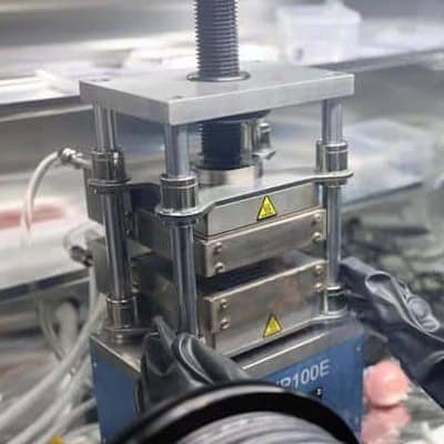
The technique developed by Guangyu Zhang, Luojun Du and colleagues involves heating powders of pure metals between two monolayer-MoS2/sapphire vdW anvils. The team used MoS2/sapphire because both materials are atomically flat and lack dangling bonds that could react with the metals. They also have high Young’s moduli, of 430 GPa and 300 GPa respectively, meaning they can withstand extremely high pressures.

Once the metal powders melted into a droplet, the researchers applied a pressure of 200 MPa. They then continued this “vdW squeezing” until the opposite sides of the anvils cooled to room temperature and 2D sheets of metal formed.

The team produced five atomically thin 2D metals using this technique. The thinnest, at around 5.8 Å, was tin, followed by bismuth (~6.3 Å), lead (~7.5 Å), indium (~8.4 Å) and gallium (~9.2 Å).

“Arduous explorations”

Zhang, Du and colleagues started this project around 10 years ago after they decided it would be interesting to work on 2D materials other than graphene and its layered vdW cousins. At first, they had little success. “Since 2015, we tried out a host of techniques, including using a hammer to thin a metal foil – a technique that we borrowed from gold foil production processes – all to no avail,” Du recalls. “We were not even able to make micron-thick foils using these techniques.”

After 10 years of what Du calls “arduous explorations”, the team finally moved a crucial step forward by developing the vdW squeezing method.

Writing in Nature, the researchers say that the five 2D metals they’ve realized so far are just the “tip of the iceberg” for their method. They now intend to increase this number. “In terms of novel properties, there is still a knowledge gap in the emerging electrical, optical, magnetic properties of 2D metals, so it would be nice to see how these materials behave physically as compared to their bulk counterparts thanks to 2D confinement effects,” says Zhang. “We would also like to investigate to what extent such 2D metals could be used for specific applications in various technological fields.”

The post Two-dimensional metals make their debut appeared first on Physics World.

  •  

Designer van der Waals materials for quantum optical emission

Join us for an insightful webinar highlighting cutting-edge research in 2D transition-metal dichalcogenides (TMDs) and their applications in quantum optics.

This session will showcase multimodal imaging techniques, including reflection and time-resolved photoluminescence (TRPL), performed with our high-performance MicroTime 100 microscope. Complementary spectroscopic insights are provided through photoluminescence emission measurements using the FluoTime 300 spectrometer, highlighting the unique characteristics of these advanced materials and their potential in next-generation photonic devices.

Whether you’re a researcher, engineer, or enthusiast in nanophotonics and quantum materials, this webinar will offer valuable insights into the characterization and design of van der Waals materials for quantum optical applications. Don’t miss this opportunity to explore the forefront of 2D material spectroscopy and imaging with a leading expert in the field.

Shengxi Huang
Shengxi Huang

Shengxi Huang is an associate professor in the Department of Electrical and Computer Engineering at Rice University. Huang earned her PhD in electrical engineering and computer science at MIT in 2017, under the supervision of Professors Mildred Dresselhaus and Jing Kong. Following that, she did postdoctoral research at Stanford University with Professors Tony Heinz and Jonathan Fan. She obtained her bachelor’s degree with the highest honors at Tsinghua University, China. Before joining Rice, she was an assistant professor in the Department of Electrical Engineering, Department of Biomedical Engineering, and Materials Research Institute at The Pennsylvania State University.

Huang’s research interests involve light-matter interactions of quantum materials and nanostructures, and the development of new quantum optical platforms and biochemical sensing technologies. In particular, her research focuses on (1) understanding optical and electronic properties of new materials such as 2D materials and Weyl semimetals, (2) developing new biochemical sensing techniques with applications in medical diagnosis, and (3) exploring new quantum optical effects and quantum sensing. She is leading the SCOPE (Sensing, Characterization, and OPtoElectronics) Laboratory.

The post Designer van der Waals materials for quantum optical emission appeared first on Physics World.

  •