Achieving a profound understanding of any subject is hard. When that subject is quantum mechanics, it’s even harder. And when one departs from ideal theoretical scenarios and enters the real world of experimental limitations, it becomes more challenging still – yet that is what physicists at the Freie Universität Berlin (FU-Berlin), Germany recently did by exploring what happens to entanglement theory in real quantum computers. In doing so, they created a bridge between two fields that have so far largely developed in parallel: entanglement theory (rooted in physics) and computational complexity (rooted in computer science).
Ebits, the standard currency of entanglement
In quantum mechanics, a composite system is said to be entangled when its total wavefunction cannot be written as a product of the states of its individual subsystems. This leads to correlations between subsystems that arise from the structure of the quantum state, not from any shared classical information. Many speed-ups achieved in quantum computing, quantum cryptography and quantum metrology rely heavily on entanglement, but not every form of entanglement is equally useful. Only specific kinds of entanglement will enable a given computational or communication task.
To make quantum technologies practical, the available entangled resources must therefore often be converted into forms suitable for specific applications. One major conversion process involves transforming partially entangled states into, or extracting them from, the maximally entangled bit (ebit) that acts as the standard unit of entanglement. High-fidelity ebits – entangled pairs that are extremely close to the ideal perfectly entangled state – can be distilled from noisy or imperfect entangled states through entanglement distillation, while entanglement dilution allows one to reconstruct the desired entangled states from purified ebits.
In an idealized setting, with an infinite number of copies of entangled states and unlimited computational power, a single quantity called the von Neumann entropy fully determines how many ebits can be extracted or are required. But reality is far less forgiving: we never have infinite resources, and computational power is always limited, just like we don’t have an infinite amount of gold on Earth.
Entanglement under finite resources
In the present work, which is published in Nature Physics, the FU-Berlin team of Lorenzo Leone, Jacopo Rizzo, Jens Eisert and Sofiene Jerbi asked what happens when these ideal assumptions break down. They study the case where only a finite number of entangled states, which can scale at most polynomially with the number of quantum bits (qubits) in the system, are considered and all local operations and classical communication (LOCC) are performed in a finite polynomial time.
They found that the simple correspondence between von Neumann entropy and extractable or required ebits no longer holds: even when a state has a large von Neumann entropy, the number of ebits that can be efficiently extracted may be much lower. In these cases, the number is bounded instead by the min-entropy of the reduced state (an operational measure determined solely by the state’s largest eigenvalue that captures how much entanglement can be reliably distilled from a single copy of the state) without averaging over many uses. On the other hand, even a state with negligible von Neumann entanglement may require a maximal ebit budget for efficient dilution.
Leone and Eisert say they were inspired to perform this study by recent work on so-called pseudo-entangled states, which are states that look at lot more entangled than they are for computationally bounded observers. Their construction of pseudo-entangled states highlights a dramatic worst-case scenario: a state that appears almost unentangled by conventional measures may still require a large number of ebits to create it efficiently. The takeaway is that computability matters, and quantum resources you might have thought were available may be, in effect, locked away simply because they cannot be processed efficiently. In other words, practical limitations make the line between a “resource” and a “usable resource” even sharper.
Quantum resources in a limited world
The researchers say that their study raises multiple questions for future exploration. One such question concerns whether a similar computational‐efficiency gap exists for other quantum resources such as magic and coherence. Another is whether one can build a full resource theory with complexity constraints, where quantities reflect not just what can be converted, but how efficient that conversion is.
Regardless of the answers, the era of entanglement under infinite book‐keeping is giving way to an era of entanglement under limited books, limited clocks and limited gates. And in this more realistic space, quantum technologies may still shine, but the calculus of what can be done and what can be harnessed needs a serious retooling.
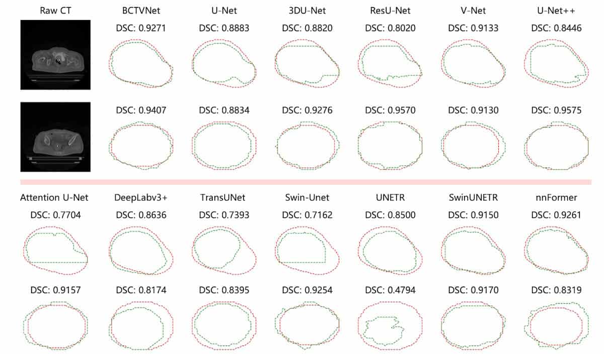
CTV segmentation test Target contouring in two example slices of a patient’s CT scan, using BCTVNet and 12 comparison models. Red and green contours represent the ground truth and the model predictions, respectively. Each image is annotated with the corresponding Dice similarity coefficient. (Courtesy: CC BY 4.0/Mach. Learn.: Sci. Technol. 10.1088/2632-2153/ae2233
Brachytherapy – a cancer treatment that destroys tumours using small radioactive sources implanted inside the body – plays a critical role in treating cervical cancer, offering an important option for patients with inoperable locally advanced disease. Brachytherapy can deliver high radiation doses directly to the tumour while ensuring nearby healthy tissues receive minimal dose; but its effectiveness relies on accurate delineation of the treatment target. A research team in China is using a hybrid deep-learning model to help with this task.
Planning brachytherapy treatments requires accurate contouring of the clinical target volume (CTV) on a CT scan, a task that’s traditionally performed manually. The limited soft-tissue contrast of CT, however, can result in unclear target boundaries, while applicator or needle insertion (used to deliver the radioactive sources) can deform and displace nearby organs. This makes manual contouring a time-consuming and subjective task that requires a high level of operator expertise.
Automating this process could reduce reliance on operator experience, increase workflow efficiency and improve contouring consistency. With this aim, the research team – headed up by He Ma from Northeastern University and Lin Zhang from Shanghai University of International Business and Economics – developed a 3D hybrid neural network called BCTVNet.
Currently, most brachytherapy segmentation models are based on convolutional neural networks (CNNs). CNNs effectively capture local structural features and can model fine anatomical details but struggle with long-range dependencies, which can cause problems if the target extends across multiple CT slices. Another option is to use transformer-based models that can integrate spatial information across distant regions and slices; but these are less effective at capturing fine-grained local detail.
To combine the strengths of both, BCTVNet integrates CNN with transformer branches to provide strong local detail extraction along with global information integration. BCTVNet performs 3D segmentation directly on post-insertion CT images, enabling the CTV to be defined based on the actual treatment geometry.
Model comparisons
Zhang, Ma and colleagues assessed the performance of BCTVNet using a private CT dataset from 95 patients diagnosed with locally advanced cervical cancer and treated with CT-guided 3D brachytherapy (76 in the training set, 19 in the test set). The scans had an average of 96 slices per patient and a slice thickness of 3 mm.
CT scans used to plan cervical cancer brachytherapy often exhibit unclear target boundaries. To enhance the local soft-tissue contrast and improve boundary recognition, the researchers pre-processed the CT volumes with a 3D version of the CLAHE (contrast-limited adaptive histogram equalization) algorithm, which processes the entire CT scan as a volumetric input. They then normalized the intensity values to standardize the input for the segmentation models.
The researchers compared BCTVNet with 12 popular CNN- and transformer-based segmentation models, evaluating segmentation performance via a series of metrics, including Dice similarity coefficient (DSC), Jaccard index, Hausdorff distance 95th percentile (HD95) and average surface distance.
Contours generated by BCTVNet were closest to the ground truth, reaching a DSC of 83.24% and a HD95 (maximum distance from ground truth excluding the worst 5%) of 3.53 mm. BCTVNet consistently outperformed the other models across all evaluation metrics. It also demonstrated strong classification accuracy, with a precision of 82.10% and a recall of 85.84%, implying fewer false detections and successful capture of target regions.
To evaluate the model’s generalizability, the team conducted additional experiments on the public dataset SegTHOR, which contains 60 thoracic 3D CT scans (40 for training, 20 for testing) from patients with oesophageal cancer. Here again, BCTVNet achieved the best scores among all the segmentation models, with the highest average DSC of 87.09% and the lowest average HD95 of 7.39 mm.
“BCTVNet effectively overcomes key challenges in CTV segmentation and achieves superior performance compared to existing methods,” the team concludes. “The proposed approach provides an effective and reliable solution for automatic CTV delineation and can serve as a supportive tool in clinical workflows.”
Under pressure A researcher in Beijing operates an apparatus used to make 2D metals. (Courtesy: CAS IOP/Handout via Xinhua)
The Physics World 2025 Breakthrough of the Year is awarded to Guangyu Zhang, Luojun Du and colleagues at the Institute of Physics of the Chinese Academy of Sciences for producing the first 2D sheets of metal. The team produced five atomically thin 2D metals – bismuth, tin, lead, indium and gallium – with the thinnest being around 6.3 Å. The researchers say their work is just the “tip of the iceberg” and now aim to use their new materials to probe the fundamentals of physics. Their breakthrough could also lead to the development of new technologies.
Since the discovery of graphene – a sheet of carbon just one atom thick – in 2004, hundreds of other 2D materials have been fabricated and studied. In most of these, layers of covalently bonded atoms are separated by gaps where neighbouring layers are held together only by weak van der Waals (vdW) interactions, making it relatively easy to “shave off” single layers to make 2D sheets. Many thought that making atomically thin metals would be impossible given that each atom in a metal is strongly bonded to surrounding atoms in all directions.
The technique developed by Zhang, Du and colleagues involves heating powders of pure metals between two monolayer-MoS2/sapphire vdW anvils. Once the metal powders are melted into a droplet, the researchers applied a pressure of 200 MPa and continued this “vdW squeezing” until the opposite sides of the anvils cooled to room temperature and 2D sheets of metal were formed.
“Right now, we have reported five single element metals, but actually we can do more because of the 88 metals in the periodic table,” Zhang explains in today’s episode of the Physics World Weekly podcast. In the podcast, he also talks about the team’s motivation creating 2D metals and some of the possible technological applications of the materials.
The Breakthrough of the Year was chosen by the Physics World editorial team. We looked back at all the scientific discoveries we have reported on since 1 January and picked the most important. In addition to being reported in Physics World in 2025, the breakthrough must meet the following criteria:
Significant advance in knowledge or understanding
Importance of work for scientific progress and/or development of real-world applications
Of general interest to Physics World readers
Before we picked our winners, we released the Physics World Top 10 Breakthroughs for 2025, which served as our shortlist. The other nine breakthroughs are listed below in no particular order.
Analysing returned samples Tim McCoy (right), curator of meteorites at the Smithsonian’s National Museum of Natural History, and research geologist Cari Corrigan examine scanning electron microscope (SEM) images of a Bennu sample. (Courtesy: James Di Loreto, Smithsonian)
To Tim McCoy, Sara Russell, Danny Glavin, Jason Dworkin, Yoshihiro Furukawa, Ann Nguyen, Scott Sandford, Zack Gainsforth and an international team of collaborators for identifying salt, ammonia, sugar, nitrogen- and oxygen-rich organic materials, and traces of metal-rich supernova dust, in samples returned from the near-Earth asteroid 101955 Bennu. The incredible chemical richness of this asteroid, which NASA’s OSIRIS-REx spacecraft visited in 2020, lends support to the longstanding hypothesis that asteroid impacts could have “seeded” the early Earth with the raw ingredients needed for life to form. The discoveries also enhance our understanding of how Bennu and other objects in the solar system formed out of the disc of material that coalesced around the young Sun.
To Takamasa Momose of the University of British Columbia, Canada, and Susumu Kuma of the RIKEN Atomic, Molecular and Optical Physics Laboratory, Japan for observing superfluidity in a molecule for the first time. Molecular hydrogen is the simplest and lightest of all molecules, and theorists predicted that it would enter a superfluid state at a temperature between 1‒2 K. But this is well below the molecule’s freezing point of 13.8 K, so Momose, Kuma and colleagues first had to develop a way to keep the hydrogen in a liquid state. Once they did that, they then had to work out how to detect the onset of superfluidity. It took them nearly 20 years, but by confining clusters of hydrogen molecules inside helium nanodroplets, embedding a methane molecule within the clusters, and monitoring the methane’s rotation, they were finally able to do it. They now plan to study larger clusters of hydrogen, with the aim of exploring the boundary between classical and quantum behaviour in this system.
To researchers at the University of Southampton and Microsoft Azure Fiber in the UK, for developing a new type of optical fibre that reduces signal loss, boosts bandwidth and promises faster, greener communications. The team, led by Francesco Poletti, achieved this feat by replacing the glass core of a conventional fibre with air and using glass membranes that reflect light at certain frequencies back into the core to trap the light and keep it moving through the fibre’s hollow centre. Their results show that the hollow-core fibres exhibit 35% less attenuation than standard glass fibres – implying that fewer amplifiers would be needed in long cables – and increase transmission speeds by 45%. Microsoft has begun testing the new fibres in real systems, installing segments in its network and sending live traffic through them. These trials open the door to gradual rollout and Poletti suggests that the hollow-core fibres could one day replace existing undersea cables.
PAT pioneers The research team in the proton therapy gantry room. (Courtesy: UO Fisica Sanitaria and UO Protonterapia, APSS, Trento)
To Francesco Fracchiolla and colleagues at the Trento Proton Therapy Centre in Italy for delivering the first clinical treatments using proton arc therapy (PAT). Proton therapy – a precision cancer treatment – is usually performed using pencil-beam scanning to precisely paint the dose onto the tumour. But this approach can be limited by the small number of beam directions deliverable in an acceptable treatment time. PAT overcomes this by moving to an arc trajectory with protons delivered over a large number of beam angles and the potential to optimize the number of energies used for each beam direction. Working with researchers at RaySearch Laboratories in Sweden, the team performed successful dosimetric comparisons with clinical proton therapy plans. Following a feasibility test that confirmed the viability of clinical PAT delivery, the researchers used PAT to treat nine cancer patients. Importantly, all treatments were performed using the centre’s existing proton therapy system and clinical workflow.
To Peter Maurer and David Awschalom at the University of Chicago Pritzker School of Molecular Engineering and colleagues for designing a protein quantum bit (qubit) that can be produced directly inside living cells and used as a magnetic field sensor. While many of today’s quantum sensors are based on nitrogen–vacancy (NV) centres in diamond, they are large and hard to position inside living cells. Instead, the team used fluorescent proteins, which are just 3 nm in diameter and can be produced by cells at a desired location with atomic precision. These proteins possess similar optical and spin properties to those of NV centre-based qubits – namely that they have a metastable triplet state. The researchers used a near-infrared laser pulse to optically address a yellow fluorescent protein and read out its triplet spin state with up to 20% spin contrast. They then genetically modified the protein to be expressed in bacterial cells and measured signals with a contrast of up to 8%. They note that although this performance does not match that of NV quantum sensors, it could enable magnetic resonance measurements directly inside living cells, which NV centres cannot do.
To the team led by Yichao Zhang at the University of Maryland and Pinshane Huang of the University of Illinois at Urbana-Champaign for capturing the highest-resolution images ever taken of individual atoms in a material. The team used an electron-microscopy technique called electron ptychography to achieve a resolution of 15 pm, which is about 10 times smaller than the size of an atom. They studied a stack of two atomically-thin layers of tungsten diselenide, which were rotated relative to each other to create a moiré superlattice. These twisted 2D materials are of great interest to physicists because their electronic properties can change dramatically with small changes in rotation angle. The extraordinary resolution of their microscope allowed them to visualize collective vibrations in the material called moiré phasons. These are similar to phonons, but had never been observed directly until now. The team’s observations align with theoretical predictions for moiré phasons. Their microscopy technique should boost our understanding of the role that moiré phasons and other lattice vibrations play in the physics of solids. This could lead to the engineering of new and useful materials.
Exquisite control Physicist Barbara Latacz at the BASE experiment at CERN. (Courtesy: CERN)
To CERN’s BASE collaboration for being the first to perform coherent spin spectroscopy on a single antiproton – the antimatter counterpart of the proton. Their breakthrough is the most precise measurement yet of the antiproton’s magnetic properties, and could be used to test the Standard Model of particle physics. The experiment begins with the creation of high-energy antiprotons in an accelerator. These must be cooled (slowed down) to cryogenic temperatures without being lost to annihilation. Then, a single antiproton is held in an ultracold electromagnetic trap, where microwave pulses manipulate its spin state. The resulting resonance peak was 16 times narrower than previous measurements, enabling a significant leap in precision. This level of quantum control opens the door to highly sensitive comparisons of the properties of matter (protons) and antimatter (antiprotons). Unexpected differences could point to new physics beyond the Standard Model and may also reveal why there is much more matter than antimatter in the visible universe.
To Richard Allen, director of the Berkeley Seismological Laboratory at the University of California, Berkeley, and Google’s Marc Stogaitis and colleagues for creating a global network of Android smartphones that acts as an earthquake early warning system. Traditional early warning systems use networks of seismic sensors that rapidly detect earthquakes in areas close to the epicentre and issue warnings across the affected region. Building such seismic networks, however, is expensive, and many earthquake-prone regions do not have them. The researchers utilized the accelerometer in millions of phones in 98 countries to create the Android Earthquake Alert (AEA) system. Testing the app between 2021 and 2024 led to the detection of an average of 312 earthquakes a month, with magnitudes ranging from 1.9 to 7.8. For earthquakes of magnitude 4.5 or higher, the system sent “TakeAction” alerts to users, sending them, on average, 60 times per month for an average of 18 million individual alerts per month. The system also delivered lesser “BeAware” alerts to regions expected to experience a shaking intensity of magnitude 3 or 4. The team now aims to produce maps of ground shaking, which could assist the emergency response services following an earthquake.
To Lisa Nortmann at Germany’s University of Göttingen and colleagues for creating the first detailed “weather map” of an exoplanet. The forecast for exoplanet WASP-127b is brutal with winds reaching 33,000 km/hr, which is much faster than winds found anywhere in the Solar System. The WASP-127b is a gas giant located about 520 light–years from Earth and the team used the CRIRES+ instrument on the European Southern Observatory’s Very Large Telescope to observe the exoplanet as it transited across its star in less than 7 h. Spectral analysis of the starlight that filtered through WASP-127b’s atmosphere revealed Doppler shifts caused by supersonic equatorial winds. By analysing the range of Doppler shifts, the team created a rough weather map of WASP-127b, even though they could not resolve light coming from specific locations on the exoplanet. Nortmann and colleagues concluded that the exoplanet’s poles are cooler that the rest of WASP-127b, where temperatures can exceed 1000 °C. Water vapour was detected in the atmosphere, raising the possibility of exotic forms of rain.
Physics World‘s coverage of the Breakthrough of the Year is supported by Reports on Progress in Physics, which offers unparalleled visibility for your ground-breaking research.
This episode of the Physics World Weekly podcast features Guangyu Zhang. Along with his colleagues at the Institute of Physics of the Chinese Academy of Sciences, Zhang has bagged the 2025 Physics World Breakthrough of the Year award for creating the first 2D metals.
In a wide-ranging conversation, we chat about the motivation behind the team’s research; the challenges in making 2D metals and how these were overcome; and how 2D metals could be used to boost our understanding of condensed matter physics and create new technologies.
I am also joined by my Physics World colleague Matin Durrani to talk about some of the exciting physics that we will be showcasing in 2025.
Physics World‘s coverage of the Breakthrough of the Year is supported by Reports on Progress in Physics, which offers unparalleled visibility for your ground-breaking research.
Julia Sutcliffe (second from the left), Chief Scientific Advisor for the UK’s Department for Business and Trade, visits the NQCC’s experimental facilities on the Harwell Cluster (Courtesy: NQCC)
Ever since the National Quantum Computing Centre was launched five years ago, its core mission has been to accelerate the pathway towards practical adoption of the technology. That has required technical innovation to scale up hardware platforms and create the software tools and algorithms needed to tackle real-world applications, but there has also been a strong focus on engaging with companies to build connections, provide access to quantum resources, and identify opportunities for deriving near-term value from quantum computing.
It makes sense, then, that the NQCC should form the cornerstone of a new Quantum Cluster at the Harwell Campus of Science and Innovation in Oxfordshire. The hope is that the NQCC’s technical expertise and infrastructure, combined with the services and facilities available on the wider Harwell Campus, will provide a magnet for new quantum start-ups as well as overseas companies that are seeking to establish a presence within the UK’s quantum ecosystem.
By accelerating collaboration across government, industry and academia, we will turn research excellence into industrial strength.
“We want to leverage the public investment that has been made into the NQCC to catalyse business growth and attract more investment into the UK’s quantum sector,” said Najwa Sidqi, manager of the Harwell Quantum Cluster, at the official launch event in November. “By accelerating collaboration across government, industry and academia, we will turn research excellence into industrial strength.”
The cluster, which has been ramping up its activities over the last year, is working to ambitious targets. Over the next decade the aim is to incubate at least 100 quantum companies on the Harwell site, create more than 1000 skilled jobs, and generate more than £1 billion of private and public investment. “Our aim is to build the foundations of a globally competitive quantum economy that delivers impact far beyond science and research,” added Sidqi.
Tangible evidence that the approach works is offered by the previous clustering activities on the Harwell Campus, notably the Space Cluster that has expanded rapidly since its launch in 2010. Anchored by the RAL Space national laboratory and bolstered by the presence of ESA and the UK Space Agency, the Space Cluster now comprises more than 100 organizations that range from small start-ups to the UK technology hubs of global heavyweights such as Airbus and Lockheed Martin.
More generally, the survival rate of start-up companies operating on the Harwell site is around 95%, compared with an average of around 50%. “At Harwell there is a high density of innovators sharing the same space, which generates more connections and more ideas,” said Julia Sutcliffe, Chief Scientific Advisor for the UK’s Department for Business and Trade. “It provides an incredible combination of world-class infrastructure and expertise, accelerating the innovation pathway and helping to create a low-risk environment for early-stage businesses and investors.”
The NQCC has already seeded that innovation activity through its early engagement with both quantum companies and end users of the technology. One major initiative has been the testbed programme, which has enabled the NQCC to invest £30m in seven hardware companies to deploy prototype quantum computers on the Harwell Campus. As well as providing access to operational systems based on all of the leading qubit modalities, the testbed programme has also provided an impetus for inward investment and job creation.
One clear example is provided by QuEra Computing, a US-based spin-off from Harvard University and the Massachusetts Institute of Technology that is developing a hardware platform based on neutral atoms. QuEra was one of the companies to win funding through the testbed programme, with the firm setting up a UK-based team to deploy its prototype system on the Harwell Campus. But the company could soon see the benefits of establishing a UK centre for technology development on the site. “Harwell is immensely helpful to us,” said Ed Durking, Corporate Director of QuEra Computing UK. “It’s a nucleus where we enjoy access to world-class talent, vendors, customers, and suppliers.”
On a practical level, establishing its UK headquarters on the Harwell Campus has provided QueEra with easy access to specialist contractors and services for fitting out and its laboratories. In June the company moved into a building that is fully equipped with flexible lab space for R&D and manufacturing, and since then the UK-based team has started to build the company’s most powerful quantum computer at the facility. Longer term, establishing a base within the UK could open the door to new collaborations and funding opportunities for QuEra to further develop its technology, with the company now focused on integrating full error correction into its neutral-atom platform by 2026.
Access to the world-class infrastructure on the Harwell Campus has benefitted the other testbed providers in different ways. For ORCA Computing, a UK company developing and manufacturing photonic quantum computers, the goal was to install a testbed system within Harwell’s high-performance computing centre rather than the NQCC’s experimental labs. “Our focus is to build commercial photonic quantum systems that can be integrated into conventional datacentres, enabling hybrid quantum-classical workflows for real-world applications,” explained Geoff Barnes, Head of Customer Success at ORCA. “Having the NQCC as an expert customer enabled us to demonstrate and validate our capabilities, building the system in our own facility and then deploying it within an operational environment.”
This process provided a valuable learning experience for the ORCA engineers. The experts at Harwell helped them to navigate the constraints of installing equipment within a live datacentre, while also providing practical assistance with the networking infrastructure. Now that the system is up and running, the Harwell site also provides ORCA with an open environment for showcasing its technology to prospective customers. “As well as delivering a testbed system to the NQCC, we can now demonstrate our platform to clients within a real-world setting,” added Barnes. “It has also been a critical step toward commercial deployment on our roadmap, enabling our partners to access our systems remotely for applications development.”
Michael Cuthbert (left), Director of the NQCC, takes Sutcliffe and other visitors on a tour of the national lab (Courtesy: NQCC)
While the NQCC has already played a vital role in supporting companies as they make the transition towards commercialization, the Quantum Cluster has a wider remit to extend those efforts into other quantum technologies, such as sensing and communications, that are already finding real-world applications. It will also have a more specific focus on attracting new investment into the UK, and supporting the growth of companies that are transitioning from the start-up phase to establish larger scale commercial operations.
“In the UK we have traditionally been successful in creating spin-off activities from our strong research base, but it has been more challenging to generate the large capital investments needed to scale businesses in the technology sector,” commented Sidqi. “We want to strengthen that pipeline to ensure that the UK can translate its leadership in quantum research and early-stage innovation into long-term prosperity.”
To accelerate that process the Quantum Cluster announced a strategic partnership with Quantum Exponential, the first UK-based venture capital fund to be entirely focused on quantum technologies. Ian Pearson, the non-executive chairman of the Quantum Exponential, explained that the company is working to generate an investment fund of £100m by the end of 2027 that will support quantum companies as they commercialize their technologies and scale up their businesses. “Now is the time for investment into quantum sector,” said Pearson. “A specialist quantum fund with the expertise needed to analyse and price deals, and to do all the necessary due diligence, will attract more private investment that will help UK companies to grow and scale.”
Around two-thirds of the investments will be directed towards UK-based companies, and as part of the partnership Quantum Exponential will work with the Quantum Cluster to identify and support high-potential quantum businesses within the Harwell Campus. The Quantum Cluster will also play a crucial role in boosting investor confidence – particularly in the unique ability of the Harwell Campus to nurture successful technology businesses – and making connections with international innovation networks to provide UK-based companies with improved access to global markets.
“This new cluster strengthens our national capability and sends a clear signal to global investors that the UK is the place to develop and scale quantum technologies,” commented Michael Cuthbert, Director of the NQCC. “It will help to ensure that quantum innovation delivers benefits not just for science and industry, but for the economy and society as a whole.”
An aerogel material that is more than 99% transparent to light and is an excellent thermal insulator has been developed by Ivan Smalyukh and colleagues at the University of Colorado Boulder in the US. Called MOCHI, the material can be manufactured in large slabs and could herald a major advance in energy-efficient windows.
While the insulating properties of building materials have steadily improved over the past decades, windows have consistently lagged behind. The problem is that current materials used in windows – mostly glass – have an inherent trade-off between insulating ability and optical transparency. This is addressed to some extent by using two or three layers of glass in double- and triple-glazed windows. However, windows remain the largest source of heat loss from most buildings.
A solution to the window problem could lie with aerogels in which the liquid component of a regular gel is replaced with air. This creates solid materials with networks of pores that make aerogels the lightest solid materials ever produced. If the solid component is a poor conductor of heat, then the aerogel will be an extremely good thermal insulator.
“Conventional aerogels, like the silica and cellulose based ones, are common candidates for transparent, thermally insulating materials,” Smalyukh explains. “However, their visible-range optical transparency is intrinsically limited by the scattering induced by their polydisperse pores – which can range from nanometres to micrometres in scale.”
Hazy appearance
While this problem can be overcome fairly easily in thin aerogel films, creating appropriately-sized pores on the scale of practical windows has so far proven much more difficult, leading to a hazy, translucent appearance.
Now, Smalyukh’s team has developed a new fabrication technique involving a removable template. Their approach hinges on the tendency of surfactant molecules called CPCL to self-assemble in water. Under carefully controlled conditions, the molecules spontaneously form networks of cylindrical tubes, called micelles. Once assembled, the aerogel precursor – a silicone material called polysiloxane – condenses around the micelles, freezing their structure in place.
“The ensuing networks of micelle-templated polysiloxane tubes could be then preserved upon the removal of surfactant, and replacing the fluid solvent with air,” Smalyukh describes. The end result was a consistent mesoporous structure, with pores ranging from 2–50 nm in diameter. This is too small to scatter visible light, but large enough to interfere with heat transport.
As a result, the mesoporous, optically clear heat insulator (MOCHI) maintains its transparency even when fabricated in slabs over 3 cm thick and a square metre in area. This suggests that it could be used to create practical windows.
High thermal performance
“We demonstrated thermal conductivity lower than that of still air, as well as an average light transmission above 99%,” Smalyukh says. “Therefore, MOCHI glass units can provide a similar rate of heat transfer to high-performing building roofs and walls, with thicknesses comparable to double pane windows.”
If rolled out on commercial scales, this could lead to entirely new ways to manage interior heating and cooling. According to the team’s calculations, a building retrofitted with MOCHI windows could boost its energy efficiency from around 6% (a typical value in current buildings) to over 30%, while reducing the heat energy passing through by around 50%.
With its ability to admit light while blocking heat transport, the researchers suggest that MOCHI could unlock entirely new functionalities for conventional windows. “Such transparent insulation also allows for efficient harnessing of thermal energy from unconcentrated solar radiation in different climate zones, promising the use of parts of opaque building envelopes as solar thermal energy generating panels,” Smalyukh adds.
Errors are the bugbear of quantum computing, and they’re hard to avoid. While quantum computers derive their computational clout from the fact that their qubits can simultaneously court multiple values, the fragility of qubit states ramps up their error rates. Many research groups are therefore seeking to reduce or manage errors so they can increase the number of qubits without reducing the whole enterprise to gibberish.
A team at the US-based firm Atom Computing is now reporting substantial success in this area thanks to a multi-part strategy for keeping large numbers of qubits operational in quantum processors based on neutral atoms. “These capabilities allow for the execution of more complex, longer circuits that are not possible without them,” says Matt Norcia, one of the Atom Computing researchers behind this work.
While neutral atoms offer several advantages over other qubit types, they traditionally have significant drawbacks for one of the most common approaches to error correction. In this approach, some of the entangled qubits are set aside as so-called “ancillaries”, used for mid-circuit measurements that can indicate how a computation is going and what error correction interventions may be necessary.
In neutral-atom quantum computing, however, such interventions are generally destructive. Atoms that are not in their designated state are simply binned off – a profligate approach that makes it challenging to scale up atom-based computers. The tendency to discard atoms is particularly awkward because the traps that confine atoms are already prone to losing atoms, which introduces additional errors while reducing the number of atoms available for computations.
Reduce, re-use, replenish
As well as demonstrating protocols for performing measurements to detect errors in quantum circuits with little atom loss, the researchers at Atom Computing also showed they could re-use ancillary atoms – a double-pronged way of retaining more atoms for calculations. In addition, they demonstrated that they could replenish the register of atoms for the computation from a spatially separated stash in a magneto-optic trap without compromising the quantum state of the atoms already in the register.
Norcia says that these achievements — replacing atoms from a continuous source, while reducing the number of atoms needing replacement to begin with — are key to running computations without running out of atoms. “To our knowledge, any useful quantum computations will require the execution of many layers of gates, which will not be possible unless the atom number can be maintained at a steady-state level throughout the computation,” he tells Physics World.
Cool and spaced out
Norcia and his collaborators at Microsoft Quantum, the Colorado School of Mines and Stanford University worked with ytterbium (Yb) atoms, which he describes as “natural qubits” since they have two ground states. A further advantage is that the transitions between these qubit states and other states used for imaging and cooling are weak, meaning the researchers could couple just one qubit state to these other states at a time. The team also leveraged a previously-developed approach for mid-circuit measurement that scatters light from only one qubit state and does not disturb the other, making it less destructive.
Still, Norcia tells Physics World, “the challenge was to re-use atoms, and key to this was cooling and performance.” To this end, they first had to shift the atoms undergoing mid-circuit measurements away from the atoms in the computational register, to avoid scattering laser light off the latter. They further avoided laser-related collateral damage by designing the register such that the measurement and cooling light was not at the resonant wavelength of the register atoms. Next, they demonstrated they could cool already-measured atoms for re-use in the calculation. Finally, they showed they could non-disruptively replenish these atoms with others from a magneto-optical trap positioned 300 nm below the tweezer arrays that held atoms for the computational register.
Mikhail Lukin, a physicist at Harvard University, US who has also worked on the challenges of atom loss and re-use in scalable, fault-tolerant neutral atom computing, has likewise recently reported successful atom re-use and diminished atom loss. Although Lukin’s work differs from that of the Atom Computing team in various ways – using rubidium instead of ytterbium atoms and a different approach for low atom loss mid-circuit measurements, for starters – he says that the work by Norcia and his team “represents an important technical advance for the Yb quantum computing platform, complementing major progress in the neutral atom quantum computing community in 2025”.
The latest episode of Physics World Stories takes you inside CUWiP+, the Conference for Undergraduate Women and Non-Binary Physicists, and the role the annual event plays in shaping early experiences of studying physics.
The episode features June McCombie from the University of Nottingham, who discusses what happens at CUWiP+ events and why they are so important for improving the retention of women and non-binary students in STEM. She reflects on how the conferences create space for students to explore career paths, build confidence and see themselves as part of the physics community.
Reflections and tips from CUWiP+ 2025
University of Birmingham students Tanshpreet Kaur and Harriett McCormick share their experiences of attending the 2025 CUWiP+ event at the University of Warwick and explain why they are excited for the next event, set for Birmingham, 19–22 March 2026. They describe standout moments from 2025, including being starstruck at meeting Dame Jocelyn Bell Burnell, who discovered radio pulsars in 1967.
The episode provides practical advice to get the most out of the event. Organizers design the programme to cater for all personalities – whether you thrive in lively, social situations, or prefer time to step back and reflect. Either way, CUWiP+ offers opportunities to be inspired and to make meaningful connections.
Hosted by Andrew Glester, the episode highlights how shared experiences and supportive networks can balance the often-solitary nature of studying physics, especially when you feel excluded from the majority group.
Quantum physics, kung-fu, LEGO and singing are probably not things you would normally put together. But that’s exactly what happened at this year’s Quantum Carousel.
The event is a free variety show where incredible performers from across academia and industry converge for an evening of science communication. Held in Bristol, UK, on 14 November 2025, this was the second year the event was run – and once again it was entirely sold out.
As organizers, our goal was to bring together those involved in quantum and adjacent fields for an evening of learning and laughter. Each act was only seven minutes long and audience participation was encouraged, with questions saved for the dinner and drinks intervals.
All together now Speakers at Quantum Carousel 2025, which was organized by Zulekha Samiullah (second from right) and Hugh Barrett (far right). (Courtesy: Yolan Ankaine)
The evening kicked off with a rousing speech and song from Chris Stewart, motivating the promotion of science communication and understanding. Felix Flicker related electron spin rotations to armlocks, with a terrific demonstration on volunteer Tony Short, while Michael Berry entertained us all with his eye-opening talk on how quantum physics has democratized music.
PhD student double act Eesa Ali and Sebastien Bisdee then welcomed volunteers to the stage to see who could align a laser fastest. Maria Violaris expertly taught us the fundamentals of quantum error correction using LEGO.
Mike Shubrook explained the quantum thermodynamics of beer through stand-up comedy. And finally, John Rarity and his assistant Hugh Barrett (event co-organizer and co-author of this article) rounded off the night by demonstrating the magic of entanglement.
Our event sponsors introduced the food and drinks portions of the evening, with Antonia Seymour (chief executive of IOP Publishing) and Matin Durrani (editor-in-chief of Physics World)opening the dinner interval, while Josh Silverstone (founder and chief executive of Hartley Ultrafast) kickstarted the networking drinks reception.
Singing praises
Whether it was singing along to an acoustic guitar or rotating hands to emulate electron spin, everyone got involved, and feedback cited audience participation as a highlight.
“The event ran very smoothly, it was lots of fun and a great chance to network in a relaxed atmosphere,” said one attendee. Another added: “The atmosphere was really fun, and it was a really nice event to get loads of the quantum community together in an enjoyable setting.”
Appreciation of the atmosphere went both ways, with one speaker saying that their favourite part of the night was that “the audience was very inviting and easy to perform to”.
Audience members also enjoyed developing a better understanding of the science that drives their industry. “I understood it and I don’t have any background in physics,” said one attendee. “I feel a marker of being a good scientist is being able to explain it in layperson’s terms.”
Reaching out
With the quantum community rapidly expanding, it needs people from a wide range of backgrounds such as computer science, engineering and business. Quantum Carousel was designed to strike a balance between high-level academic discussion and entertainment through entry-level talks, such as explaining error correction with props, or relating research to impact from stimulated emission to CDs.
By focusing on real-world analogies, these talks can help newcomers to develop an intuitive and memorable understanding. Meanwhile, those already in the field can equip themselves with new ways of communicating elements of their research.
We look forward to hosting Quantum Carousel again in the future. We want to make it bigger and better, with an even greater range of diverse acts.
But if you’re interested in organizing a similar outreach event of your own, it helps to consider how you can create an environment that can best spark connections between both speakers and attendees. Consider your audience and how your event can attract different people for different reasons. In our case, this included the chance to network, engage with the performances, and enjoy the food and drink.
Quantum Carousel was founded by Zulekha Samiullah in 2024, and she and Hugh Barrett now co-lead the event. Quantum Carousel 2025 was sponsored by the QE-CDT, IOP Publishing and Hartley Ultrafast.
Scaling up The IBS Center for Van der Waals Quantum Solids (IBS-VdWQS) acts as a catalyst for advances in fundamental materials science and condensed-matter physics. The purpose-built facility is colocated on the campus of POSTECH, one of Korea’s leading universities. (Courtesy: IBS)
Our multidisciplinary team aims to create heteroepitaxial van der Waals quantum solids at system scales, where the crystal lattices and symmetries of these novel 2D materials are artificially moulded to atomic precision via epitaxial growth. Over time, we also hope to translate these new solids into quantum device platforms.
Clearly there’s all sorts of exotic materials physics within that remit.
Correct. We form van der Waals heterostructures by epitaxial manipulation of the crystal lattice in diverse, atomically thin 2D materials – for example, 2D heterostructures incorporating graphene, boron nitride or transition-metal dichalcogenides (such as MoS2, WSe2, NbSe2, TaSe2 and so on). Crucially, the material layers are held in place only by weak van der Waals forces and with no dangling chemical bonds in the direction normal to the layers.
These 2D layers can also be laterally “stitched” into hexagonal or honeycomb lattices, with the electronic and atomic motions confined into the atomic layers. Using state-of-the-art epitaxial techniques, our team can then artificially stack these lattices to form a new class of condensed matter with exotic interlayer couplings and emergent electronic, optical and magnetic properties – properties that, we hope, will find applications in next-generation quantum devices.
Moon-Ho Jo “While the focus is very much on basic science, epitaxial scalability is hard-wired into all our lines of enquiry.” (Courtesy: IBS)
The IBS headquarters was established in 2011 as Korea’s first dedicated institute for fundamental science. It’s an umbrella organization coordinating the activity of 38 centres-of-excellence across the physical sciences, life sciences, as well as mathematics and data science. In this way, IBS specializes in long-range initiatives that require large groups of researchers from Korea and abroad.
Our IBS-VdWQS is a catalyst for advances in fundamental materials science and condensed-matter physics, essentially positioned as a central-government-funded research institution in a research-oriented university. Particularly important in this regard is our colocation on the campus of Pohang University of Science and Technology (POSTECH), one of Korea’s leading academic centres, and our adjacency to large-scale facilities like the Pohang Synchrotron Radiation Facility (PAL) and Pohang X-ray free-electron laser (PAL-XFEL). It’s worth noting as well that all the principal investigators (PIs) in our centre hold dual positions as IBS researchers and POSTECH professors.
So IBS is majoring on strategic research initiatives?
Absolutely – and that perspective also underpins our funding model. The IBS-VdWQS was launched in 2022 and is funded by IBS for an initial period through to 2032 (with a series of six-year extensions subject to the originality and impact of our research). As such, we are able to encourage autonomy across our 2D materials programme, giving scientists the academic freedom to pursue questions in basic research without the bureaucracy and overhead of endless grant proposals. Team members know that, with plenty of hard work and creativity, they have everything they need here to do great science and build their careers.
Your core remit is fundamental science, but what technologies could eventually emerge from the IBS-VdWQS research programme?
While the focus is very much on basic science, epitaxial scalability is hard-wired into all our lines of enquiry. In short: we are creating new 2D materials via epitaxial growth and this ultimately opens a pathway to wafer-scale industrial production of van der Waals materials with commercially interesting semiconducting, superconducting or emergent properties in general.
Right now, we are investigating van der Waals semiconductors and the potential integration of MoS2 and WSe2 with silicon for new generations of low-power logic circuitry. On a longer timeline, we are developing new types of high-Tc (around 10 K) van der Waals superconductors for applications in Josephson junctions, which are core building blocks in superconducting quantum computers.
There’s a parallel opportunity in photonic quantum computing, with van der Waals materials shaping up as promising candidates for quantum light-emitters that generate on-demand (deterministic) and highly coherent (indistinguishable) single-photon streams.
Establishing a new research centre from scratch can’t have been easy. How are things progressing?
It’s been a busy three years since the launch of the IBS-VdWQS. The most important task at the outset was centralization – pulling together previously scattered resources, equipment and staff from around the POSTECH campus. We completed the move into our purpose-built facility, next door to the PAL synchrotron light source, at the end of last year and have now established dedicated laboratory areas for the van der Waals Epitaxy Division; Quantum Device and Optics Division; Quantum Device Fabrication Division; and the Imaging and Spectroscopy Division.
One of our front-line research efforts is building a van der Waals Quantum Solid Cluster, an integrated system of multiple instruments connected by ultra-high-vacuum lines to maintain atomically clean surfaces. We believe this advanced capability will allow us to reliably study air-sensitive van der Waals materials and open up opportunities to discover new physics in previously inaccessible van der Waals platforms.
Integrated thinking The IBS-VdWQS hosts an end-to-end research programme spanning advanced fabrication, materials characterization and theoretical studies. From left to right: vapour-phase van der Waals crystal growth; femtosecond laser spectroscopy for studying ultrafast charge, spin and lattice dynamics; and an STM system for investigations of electronic structure and local quantum properties in van der Waals materials. (Courtesy: IBS)
Are there plans to scale the IBS-VdWQS work programme?
Right now, my priority is to promote opportunities for graduate students, postdoctoral researchers and research fellows to accelerate the centre’s expanding research brief. Diversity is strength, so I’m especially keen to encourage more in-bound applications from talented experimental and theoretical physicists in Europe and North America. Our current research cohort comprises 30+ PhD students, seven postdocs (from the US, India, China and Korea) and seven PIs.
Over the next five years, we aim to scale up to 25+ postdocs and research fellows and push out in new directions such as scalable quantum devices. In particular, we are looking for scientists with specialist know-how and expertise in areas like materials synthesis, quantum transport, optical spectroscopy and scanning probe microscopy (SPM) to accelerate our materials research.
How do you support your early-career researchers at IBS-VdWQS?
We are committed to nurturing global early-career talent and provide a clear development pathway from PhD through postdoctoral studies to student research fellow and research fellow/PI. Our current staff PIs have diverse academic backgrounds – materials science, physics, electronic engineering and chemistry – and we therefore allow early-career scientists to have a nominated co-adviser alongside their main PI. This model means research students learn in an integrated fashion that encourages a “multidisciplinarian” mindset – majoring in epitaxial growth, low-temperature electronic devices and optical spectroscopy, say, while also maintaining a watching brief (through their co-adviser) on the latest advances in materials characterization and analysis.
What does success look like at the end of the current funding cycle?
With 2032 as the first milestone year in this budget cycle, we are working to establish a global hub for van der Waals materials science – a highly collaborative and integrated research programme spanning advanced fabrication, materials characterization/analysis and theoretical studies. More capacity, more research infrastructure, more international scientists are all key to delivering our development roadmap for 2D semiconductor and superconductor integration towards scalable, next-generation low-power electronics and quantum computing devices.
Myungchul Oh “We are exploring the microscopic nature of quantum materials and their device applications.” (Courtesy: IBS)
Myungchul Oh joined the IBS-VdWQS in 2023 after a five-year stint as a postdoctoral physicist at Princeton University in the US, where he studied strongly correlated phenomena, superconductivity and topological properties in “twisted” graphene systems.
Recruited as an IBS-POSTECH research fellow, Oh holds dual academic positions: team leader for the quantum-device microscopy investigations at IBS-VdWQS and assistant professor in the semiconductor engineering department at POSTECH.
Van der Waals heterostructures, assembled layer-by-layer from 2D materials, enable precise engineering of quantum properties through the interaction between different atomic layers. By extension, Oh and his colleagues are focused on the development of novel van der Waals systems; their integration into devices via nanofabrication; and the study of electrical, magnetic and topological properties under extreme conditions, where quantum-mechanical effects dominate.
“We are exploring the microscopic nature of quantum materials and their device applications,” Oh explains. “Our research combines novel 2D van der Waals heterostructure device fabrication techniques with cryogenic scanning probe microscopy (SPM) measurements – the latter to access the atomic-scale electronic structure and local physical properties of quantum phases in 2D materials.”
Atoms in a one-dimensional quantum gas behave like a Newton’s cradle toy, transferring energy from atom to atom without dissipation. Developed by researchers at the TU Wien, Austria, this quantum fluid of ultracold, confined rubidium atoms can be used to simulate more complex solid-state systems. By measuring transport quantities within this “perfect” atomic system, the team hope to obtain a deeper understanding of how transport phenomena and thermodynamics behave at the quantum level.
Physical systems transport energy, charge and mass in various ways. Electrical currents streaming along a wire, heat flowing through a solid and light travelling down an optical fibre are just three examples. How easily these quantities move inside a material depends on the resistance they experience, with collisions and friction slowing them down and making them fade away. This level of resistance largely determines whether the material is classed as an insulator, a conductor or a superconductor.
The mechanisms behind such transport fall into two main categories. The first is ballistic transport, which features linear movement without loss, like a bullet travelling in a straight line. The second is diffusive transport, where the quantity is subject to many random collisions. A good example is heat conduction, where the heat moves through a material gradually, travelling in many directions at once.
Breaking the rules
Most systems are strongly affected by diffusion, which makes it surprising that the TU Wien researchers could build an atomic system where mass and energy flowed freely without it. According to study leader Frederik Møller, the key to this unusual behaviour is the magnetic and optical fields that keep the rubidium atoms confined to one dimension, “freezing out” interactions in the atoms’ two transverse directions.
Because the atoms can only move along a single direction, Møller explains, they transfer momentum perfectly, without scattering their energy as would be the case in normal matter. Consequently, the 1D atomic system does not thermalize despite being subject to thousands of collisions.
To quantify the transport of mass (charge) and energy within this system, the researchers measured quantities known as Drude weights, which are fundamental parameters that describe ballistic, dissipationless transport in solid-state environments. According to these measurements, the single-dimensional interacting bosonic atoms do indeed demonstrate perfect dissipationless transport. The results also agree with the generalized hydrodynamics (GHD) theoretical framework, which describes the large-scale, inhomogeneous dynamics of one-dimensional integrable quantum many-body systems such as ultracold atomic gases or specific spin chains.
A Newton’s cradle for atoms
According to team leader Jörg Schmiedmayer, the experiment is analogous to a Newton’s cradle toy, which consists of a row of metal balls suspended on wires (see below). When the ball on one end of the row is made to collide with the one next to it, its momentum transfers straight through the other balls to the ball on the opposite end, which swings out. Schmiedmayer adds that the system makes it possible to study transport under perfectly controlled conditions and could open new ways of understanding how resistance emerges, or disappears, at the quantum level. “Our next steps are applying the method to strongly correlated transport and to transport in a topological fluid,” he tells Physics World.
Karèn Kheruntsyan, a theoretical physicist at the University of Queensland, Australia, who was not involved in this research, calls it “a significant step for studying quantum transport”. He says the team’s work clearly demonstrates ballistic (dissipationless) transport at a finite temperature, providing an experimental benchmark for theories of integrability and disorder. The work also validates the thermodynamic meaning of Drude weights, while confirming that linear-response theory and GHD accurately describe transport in quantum systems.
In Kheruntsyan’s view, though, the team’s biggest achievement is the quantitative extraction of Drude weights that characterize atomic and energy currents, with “excellent agreement” between experiment and theory. This, he says, shows truly ballistic transport in an interacting many-body system. One caveat, though, is that the system’s limited spatial resolution and near-ideal integrability prevent it from being used to explore diffusive regimes or stronger interaction effects, leaving microscopic dynamics such as dispersive shock waves unresolved.
Physics students from under-represented groups consistently report a lower sense of belonging at university than their over-represented peers. These students experience specific challenges that make them feel undervalued and excluded. Yet a strong sense of belonging has been shown to lead to improved academic performance, greater engagement in courses and better mental wellbeing. It is vital, then, that universities make changes to help eliminate these challenges.
Students are uniquely placed to describe the issues when it comes to belonging in physics. With this mind, as an undergraduate physics student with a passion for making the discipline more diverse and inclusive, I conducted focus groups with current and former physics students, interviewed experts and performed an analysis of current literature. This was part of a summer project funded by the Royal Institution and is currently being finalized for publication.
From this work it became clear that under-represented groups face many challenges to developing a strong sense of belonging in physics, but, at the same time, there are ways to improve the everyday experiences of students. When it comes to barriers, one is the widely held belief – reflected in the way physicists are depicted in the media and textbooks – that you need to be a “natural genius” to succeed in university physics. This notion hampers students from under-represented groups, who see peers from the over-represented majority appearing to grasp concepts more quickly and lecturers suggesting certain topics are “easy”.
The feeling that physics demands natural ability also arises from the so-called “weed out” culture, which is defined as courses that are intentionally designed to filter students out, reduce class sizes and diminish sense of belonging. Students who we surveyed believe that the high fail rate is caused by a disconnect between the teaching and workshops on the course and the final exam.
A third cause of this perception that you need some innate ability to succeed in physics is the attitudes and behaviour of some professors, lecturers and demonstrators. This includes casual sexist and racist behaviour; belittling students who ask for help; and acting as if they’re uninterested in teaching. Students from under-represented groups report significantly lower levels of respect and recognition from instructors, which damages their resilience and weakens sense of belonging.
Students from under-represented groups are also more likely to be isolated from their class mates and feel socially excluded from them. This means they lack a support network, leaving them with no-one to turn to when they encounter challenges. Outside the lecture theatre, students from under-represented groups typically face many microaggressions in their day-to-day university experience. These are subtle indignities or insults, unconsciously or consciously, towards minorities such as people of colour being told they “speak English very well”, male students refusing to accept women’s ideas, and the assumption that gender minorities will take on administrative roles in group projects.
Focus on the future
So what can be done? The good news is that there are many solutions to mitigate these issues and improve a sense of belonging. First, institutions should place more emphasis on small group “active learning” – which includes discussions, problem solving and peer-based learning. These pedagogical strategies have been shown to boost belonging, particularly for female students. After these active-learning sessions, non-academic, culturally sensitive social lunches can help turn “course friends” to “real friends” who choose to meet socially and can become a support network. This can help build connections within and between degree cohorts.
Another solution is for universities to invite former students to speak about their sense of belonging and how it evolved or improved throughout their degree. Hearing about struggles and learning tried-and-tested strategies to improve resilience can help students better prepare for stressful situations. Alumni are more relatable than generic messaging from the university wellbeing team.
Building closer links between students and staff also enhances a sense of belonging. It helps humanise lecturers and demonstrate that staff care about student wellbeing and success. This should be implemented by recognizing staff efforts formally so that the service roles of faculty members are formally recognized and professionalized.
Universities should also focus on hiring more diverse teaching staff, who can serve as role models, using their experiences to relate to and engage with under-represented students. Students will end up feeling more embedded within the physics community, improving both their sense of belonging and performance.
One practical way to increase diversity in hiring is for institutions to re-evaluate what they value. While securing large grants is valuable, so is advocating for equality, diversity and inclusion; public engagement; and the ability to inspire the next generation of physicists.
Another approach is to establish “departmental action teams” to find tailored solutions to unite undergraduates, postgraduates, teaching and research staff. Such teams identify issues specific to their particular university, and they can gather data through surveying the department to identify trends and recommend practical changes to boost belonging.
Implementing these measures will not only improve the sense of belonging for students from under-represented groups but also cultivate a more inclusive, diverse physics workforce. That in turn will boost the overall research culture, opening up research directions that may have previously been overlooked, and yielding stronger scientific outputs. It is crucial that we do more to support physics students from under-represented groups to create a more diverse physics community. Ultimately, it will benefit physics and society as a whole.
The gyromagnetic ratio is the ratio of a particle’s magnetic moment and its angular momentum. This value determines how a particle responds to a magnetic field. According to classical physics, muons should have a gyromagnetic ratio equal to 2. However, owing to quantum mechanics, there is a small difference between the expected gyromagnetic ratio and the observed value. This discrepancy is known as the anomalous magnetic moment.
The anomalous magnetic moment is incredibly sensitive to quantum fluctuations. It can be used to test the Standard Model of physics, and previous consistent experimental discrepancies have hinted at new physics beyond the Standard Model. The search for the anomalous magnetic moment is one of the most precise tests in modern physics.
To calculate the anomalous magnetic moment, experiments such as Fermilab’s Muon g-2 experiment have been set up where researchers measure the muon’s wobble frequency, which is caused by its magnetic moment. But effects such as hadronic vacuum polarization and hadronic light-by-light scattering cause uncertainty in the measurement. Unlike hadronic vacuum polarization, hadronic light-by-light cannot be directly extracted from experimental cross-section data, making it dependent on the model used and a significant computational challenge.
In this work, the researcher took a major step in resolving the anomalous magnetic moment of the muon. Their method calculated how the neutral pion contributes to hadronic light-by-light scattering, used domain wall fermions to preserve symmetry, employed eight different lattice configurations with variational pion masses, and introduced a pion structure function to find the key contributions in a model-independent method. The pion transition form factor was computed directly at arbitrary space-like photon momenta, and a Gegenbauer expansion was used to confirm that about 98% of the π⁰-pole contribution was determined in a model-independent way. The analysis also included finite-volume corrections and chiral and continuum extrapolations and yielded a value for the π⁰ decay width.
The development of a more accurate and model-independent anomalous magnetic moment for the muon has reduced major theoretical uncertainties and can make Standard Model precision tests more robust.
Entanglement is a phenomenon where two or more particles become linked in such a way that a measurement on one of the particles instantly influences the state of the other, no matter how far apart they are. It is a defining property of quantum mechanics, which is key to all quantum technologies and remains a serious challenge to realize in large systems.
However, a team of researchers from Sweden and Spain has recently made a large step forward in the field of ultrafast entanglement. Here, pairs of extreme ultraviolet pulses are used to exert quantum control on the attosecond timescale (a few quintillionths of a second).
Specifically, they studied ultrafast photoionisation. In this process, a high-energy light pulse hits an atom, ejecting an electron and leaving behind an ion.
This process can create entanglement between the electron and the ion in a controlled way. However, the entanglement is fragile and can be disrupted or transferred as the system evolves.
For instance, as the newly-created ion emits a photon to release energy, the entanglement shifts from the electron – ion pair to the electron–photon pair. This transfer process takes a considerable amount of time, on the scale of 10s of nanoseconds. This means that the ion-electron pair is macroscopically separated, on the centimetre scale.
The team found that during this transition, all three particles – electron, ion, and photon – are entangled together in a multipartite state.
They did this by using a mathematical tool called von Neumann entropy to track how much information is shared between all three particles.
Although this work was purely theoretical, they also proposed an experimental method to study entanglement transfer. The setup would use two synchronised free-electron laser pulses, with attosecond precision, to measure the electron’s energy and to detect if a photon was emitted. By measuring both particles in coincidence, entanglement can be detected.
The results could be generalised to other scenarios and will help us understand how quantum information can move between different particles. This brings us one small step closer to future technologies like quantum communication and computing.
Physicists searching for signs of quantum gravity have long faced a frustrating problem. Even if gravity does have a quantum nature, its effects are expected to show up only at extremely small distances, far beyond the reach of experiments. A new theoretical study by Benjamin Koch and colleagues at the Technical University of Vienna in Austria suggests a different strategy. Instead of looking for quantum gravity where space–time is tiny, the researchers argue that subtle quantum effects could influence how particles and light move across huge cosmical distances.
Their work introduces a new concept called q-desics, short for quantum-corrected paths through space–time. These paths generalize the familiar trajectories predicted by Einstein’s general theory of relativity and could, in principle, leave observable fingerprints in cosmology and astrophysics.
General relativity and quantum mechanics are two of the most successful theories in physics, yet they describe nature in radically different ways. General relativity treats gravity as the smooth curvature of space–time, while quantum mechanics governs the probabilistic behavior of particles and fields. Reconciling the two has been one of the central challenges of theoretical physics for decades.
“One side of the problem is that one has to come up with a mathematical framework that unifies quantum mechanics and general relativity in a single consistent theory,” Koch explains. “Over many decades, numerous attempts have been made by some of the most brilliant minds humanity has to offer.” Despite this effort, no approach has yet gained universal acceptance.
Deeper difficulty
There is another, perhaps deeper difficulty. “We have little to no guidance, neither from experiments nor from observations that could tell us whether we actually are heading in the right direction or not,” Koch says. Without experimental clues, many ideas about quantum gravity remain largely speculative.
That does not mean the quest lacks value. Fundamental research often pays off in unexpected ways. “We rarely know what to expect behind the next tree in the jungle of knowledge,” Koch says. “We only can look back and realize that some of the previously explored trees provided treasures of great use and others just helped us to understand things a little better.”
Almost every test of general relativity relies on a simple assumption. Light rays and freely falling particles follow specific paths, known as geodesics, determined entirely by the geometry of space–time. From gravitational lensing to planetary motion, this idea underpins how physicists interpret astronomical data.
Koch and his collaborators asked what happens to this assumption when space–time itself is treated as a quantum object. “Almost all interpretations of observational astrophysical and astronomical data rest on the assumption that in empty space light and particles travel on a path which is described by the geodesic equation,” Koch says. “We have shown that in the context of quantum gravity this equation has to be generalized.”
Generalized q-desic
The result is the q-desic equation. Instead of relying only on an averaged, classical picture of space–time, q-desics account for the underlying quantum structure more directly. In practical terms, this means that particles may follow paths that deviate slightly from those predicted by classical general relativity, even when space–time looks smooth on average.
Crucially, the team found that these deviations are not confined to tiny distances. “What makes our first results on the q-desics so interesting is that apart from these short distance effects, there are also long range effects possible, if one takes into account the existence of the cosmological constant,” Koch says.
This opens the door to possible tests using existing astronomical data. According to the study, q-desics could differ from ordinary geodesics over cosmological distances, affecting how matter and light propagate across the universe.
“The q-desics might be distinguished from geodesics at cosmological large distances,” Koch says, “which would be an observable manifestation of quantum gravity effects.”
Cosmological tensions
The researchers propose revisiting cosmological observations. “Currently, there are many tensions popping up between the Standard Model of cosmology and observed data,” Koch notes. “All these tensions are linked, one way or another, to the use of geodesics at vastly different distance scales.” The q-desic framework offers a new lens through which to examine such discrepancies.
So far, the team has explored simplified scenarios and idealized models of quantum space–time. Extending the framework to more realistic situations will require substantial effort.
“The initial work was done with one PhD student (Ali Riahina) and one colleague (Ángel Rincón),” Koch says. “There are many things to be revisited and explored that our to-do list is growing far too long for just a few people.” One immediate goal is to encourage other researchers to engage with the idea and test it in different theoretical settings.
Whether q-desics will provide an observational window into quantum gravity remains to be seen. But by shifting attention from the smallest scales to the largest structures in the cosmos, the work offers a fresh perspective on an enduring problem.
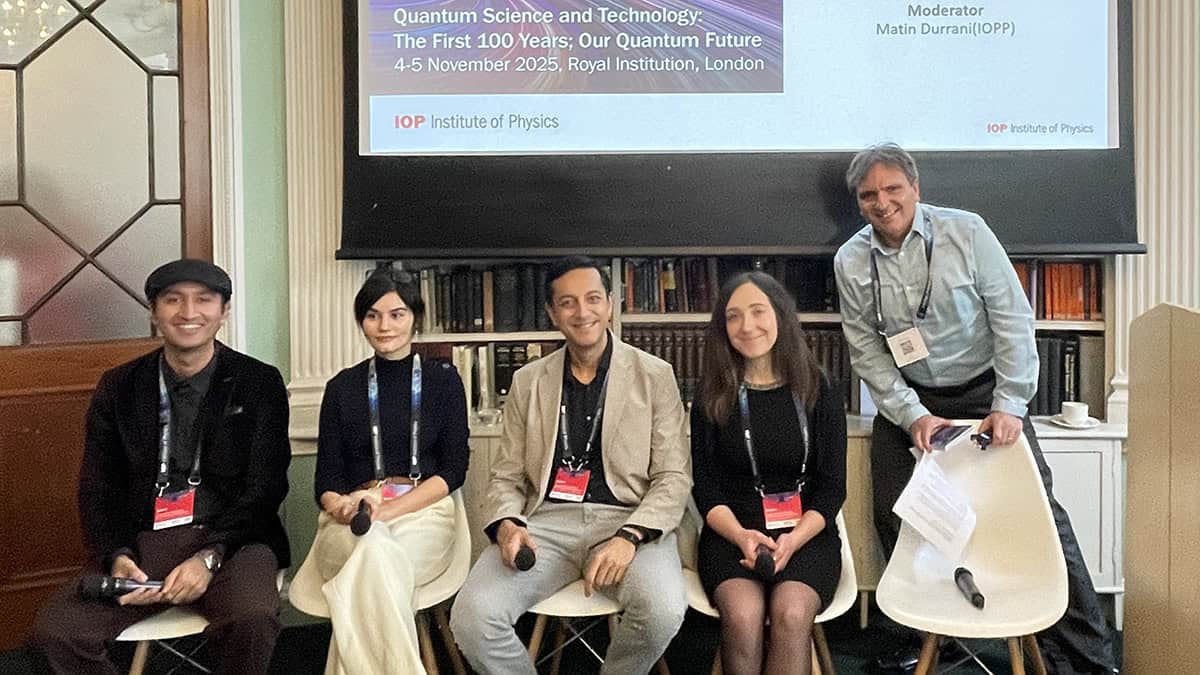
The International Year of Quantum Science and Technology has celebrated all the great developments in the sector – but what challenges and opportunities lie in store? That was the question deliberated by four future leaders in the field at the Royal Institution in central London in November. The discussion took place during the two-day conference “Quantum science and technology: the first 100 years; our quantum future”, which was part of a week-long series of quantum-related events in the UK organized by the Institute of Physics.
As well as outlining the technical challenges in their fields, the speakers all stressed the importance of developing a “skills pipeline” so that the quantum sector has enough talented people to meet its needs. Also vital will be the need to communicate the mysteries and potential of quantum technology – not just to the public but to industrialists, government officials and venture capitalists.
Two of the speakers – Nicole Gillett (Riverlane) and Muhammad Hamza Waseem (Quantinuum) – are from the quantum tech industry, with Mehul Malik (Heriot-Watt University) and Sarah Alam Malik (University College London) based in academia. The following is an edited version of the discussion.
Quantum’s future leaders
Deep thinkers The challenges and opportunities for quantum science and technology were discussed during a conference organized by the Institute of Physics at the Royal Institution on 5 November 2025 by (left to right, seated) Muhammad Hamza Waseem; Sarah Alam Malik; Mehul Malik; and Nicole Gillett. The discussion was chaired by Physics World editor-in-chief Matin Durrani (standing, far right). (Courtesy: Tushna Commissariat)
Nicole Gillett is a senior software engineer at Riverlane, in Cambridge, UK. The company is a leader in quantum error correction, which is a critical part of a fully functioning, fault-tolerant quantum computer. Errors arise because quantum bits, or qubits, are so fragile and correcting them is far trickier than with classical devices. Riverlane is therefore trying to find ways to correct for errors without disturbing a device’s quantum states. Gillett is part of a team trying to understand how best to implement error-correcting algorithms on real quantum-computing chips.
Mehul Malik, who studied physics at a liberal arts college in New York, was attracted to quantum physics because of what he calls a “weird middle ground between artistic creative thought and the rigour of physics”. After doing a PhD at the University of Rochester, he spent five years as a postdoc with Anton Zeilinger at the University of Vienna in Austria before moving to Heriot-Watt University in the UK. As head of its Beyond Binary Quantum Information research group, Malik works on quantum information processing and communication and fundamental studies of entanglement.
Sarah AlamMalik is a particle physicist at University College London, using particle colliders to detect and study potential candidates for dark matter. She is also trying to use quantum computers to speed up the discovery of new physics given that what she calls “our most cherished and compelling theories” for physics beyond the Standard Model, such as supersymmetry, have not yet been seen. In particular, Malik is trying to find new physics in a way that’s “model agnostic” – in other words, using quantum computers to search particle-collision data for anomalous events that have not been seen before.
Muhammad Hamza Waseem studied electrical engineering in Pakistan, but got hooked on quantum physics after getting involved in recreating experiments to test Bell’s inequalities in what he claims was the first quantum optics lab in the country. Waseem then moved to the the University of Oxford in the UK, to do a PhD studying spin waves to make classical and quantum logic circuits. Unable to work when his lab shut during the COVID-19 pandemic, Waseem approached Quantinuum to see if he could help them in their quest to build quantum computers using ion traps. Now based at the company, he studies how quantum computers can do natural-language processing. “Think ChatGPT, but powered with quantum computers,” he says.
What will be the biggest or most important application of quantum technology in your field over the next 10 years?
Nicole Gillett: If you look at roadmaps of quantum-computing companies, you’ll find that IBM, for example, intends to build the world’s first utility scale and fault-tolerant quantum computer by the end of the decade. Beyond 2033, they’re committing to have a system that could support 2000 “logical qubits”, which are essentially error-corrected qubits, in which the data of one qubit has been encoded into many qubits.
What can be achieved with that number of qubits is a difficult question to answer but some theorists, such as Juan Maldacena, have proposed some very exotic ideas, such as using a system of 7000 qubits to simulate black-hole dynamics. Now that might not be a particularly useful industry application, but it tells you about the potential power of a machine like this.
Mehul Malik: In my field, quantum networks that can distribute individual quantum particles or entangled states over large and short distances will have a significant impact within the next 10 years. Quantum networks will connect smaller, powerful quantum processors to make a larger quantum device, whether for computing or communication. The technology is quite mature – in fact, we’ve already got a quantum network connecting banks in London.
I will also add something slightly controversial. We often try to distinguish between quantum and non-quantum technologies, but what we’re heading towards is combining classical state-of-the-art devices with technology based on inherently quantum effects – what you might call “quantum adjacent technology”. Single-photon detectors, for example, are going to revolutionize healthcare, medical imaging and even long-distance communication.
Sarah Alam Malik: For me, the biggest impact of quantum technology will be applying quantum computing algorithms in physics. Can we quantum simulate the dynamics of, say, proton–proton collisions in a more efficient and accurate manner? Can we combine quantum computing with machine learning to sift through data and identify anomalous collisions that are beyond those expected from the Standard Model?
Quantum technology is letting us ask very fundamental questions about nature.
Sarah Alam Malik, University College London
Quantum technology, in other words, is letting us ask very fundamental questions about nature. Emerging in theoretical physics, for example, is the idea that the fundamental layer of reality may not be particles and fields, but units of quantum information. We’re looking at the world through this new quantum-theoretic lens and asking questions like, whether it’s possible to measure entanglement in top quarks and even explore Bell-type inequalities at particle colliders.
One interesting quantity is “magic”, which is a measure of how far you are from having something that can be classically simulable (Phys. Rev. D110 116016). The more magic there is in a system the less easy it is to simulate classically – and thereforethe greater the computational resource it possesses for quantum computing. We’re asking how much “magic” there is in, for instance, top quarks produced at the Large Hadron Collider. So one of the most important developments for me may well be asking questions in a very different way to before.
Muhammad Hamza Waseem: Technologically speaking, the biggest impact will be simulating quantum systems using a quantum computer. In fact, researchers from Google already claim to have simulated a wormhole in a quantum computer, albeit a very simple version that could have been tackled with a classical device (Nature612 55).
But the most significant impact has to do with education. I believe quantum theory teaches us that reality is not about particles and individuals – but relations. I’m not saying that particles don’t exist but they emerge from the relations. In fact, with colleagues at the University of Oxford, we’ve used this idea to develop a new way of teaching quantum theory, called Quantum in Pictures.
We’ve already tried our diagrammatic approach with a group of 16–18-year-olds, teaching them the entire quantum-information course that’s normally given to postgraduates at Oxford. At the end of our two-month course, which had one lecture and tutorial per week, students took an exam with questions from past Oxford papers. An amazing 80% of students passed and half got distinctions.
For quantum theory to have a big impact, we have to make quantum physics more accessible to everyone.
Muhammad Hamza Waseem, Quantinuum
I’ve also tried the same approach on pupils in Pakistan: the youngest, who was just 13, can now explain quantum teleportation and quantum entanglement. My point is that for quantum theory to have a big impact, we have to make quantum physics more accessible to everyone.
What will be the biggest challenges and difficulties over the next 10 years for people in quantum science and technology?
Nicole Gillett: The challenge will be building up a big enough quantum workforce. Sometimes people hear the words “quantum computer” and get scared, worrying they’re going to have to solve Hamiltonians all the time. But is it possible to teach students at high-school level about these concepts? Can we get the ideas across in a way that is easy to understand so people are interested and excited about quantum computing?
At Riverlane, we’ve run week-long summer workshops for the last two years, where we try to teach undergraduate students enough about quantum error correction so they can do “decoding”. That’s when you take the results of error correction and try to figure out what errors occurred on your qubits. By combining lectures and hands-on tutorials we found we could teach students about error corrections – and get them really excited too.
Our biggest challenge will be not having a workforce ready for quantum computing.
Nicole Gillett, Riverlane
We had students from physics, philosophy, maths and computer science take the course – the only pre-requisite, apart from being curious about quantum computers, is some kind of coding ability. My point is that these kinds of boot camps are going to be so important to inspire future generations. We need to make the information accessible to people because otherwise our biggest challenge will be not having a workforce ready for quantum computing.
Mehul Malik: One of the big challenges is international cooperation and collaboration. Imagine if, in the early days of the Internet, the US military had decided they’d keep it to themselves for national-security reasons or if CERN hadn’t made the World Wide Web open source. We face the same challenge today because we live in a world that’s becoming polarized and protectionist – and we don’t want that to hamper international collaboration.
Over the last few decades, quantum science has developed in a very international way and we have come so far because of that. I have lived in four different continents, but when I try to recruit internationally, I face significant hurdles from the UK government, from visa fees and so on. To really progress in quantum tech, we need to collaborate and develop science in a way that’s best for humanity not just for each nation.
Sarah Alam Malik: One of the most important challenges will be managing the hype that inevitably surrounds the field right now. We’ve already seen this with artificial intelligence (AI), which has gone though the whole hype cycle. Lots of people were initially interested, then the funding dried up when reality didn’t match expectations. But now AI has come back with such resounding force that we’re almost unprepared for all the implications of it.
Quantum can learn from the AI hype cycle, finding ways to manage expectations of what could be a very transformative technology. In the near- and mid-term, we need to not overplay things and be cautious of this potentially transformative technology – yet be braced for the impact it could potentially have. It’s a case of balancing hype with reality.
Muhammad Hamza Waseem: Another important challenge is how to distribute funding between research on applications and research on foundations. A lot of the good technology we use today emerged from foundational ideas in ways that were not foreseen by the people originally working on them. So we must ensure that foundational research gets the funding it deserves or we’ll hit a dead end at some point.
Will quantum tech alter how we do research, just as AI could do?
Mehul Malik: AI is already changing how I do research, speeding up the way I discover knowledge. Using Google Gemini, for example, I now ask my browser questions instead of searching for specific things. But you still have to verify all the information you gather, for example, by checking the links it cites. I recently asked AI a complex physics question to which I knew the answer and the solution it gave was terrible. As for how quantum is changing research, I’m less sure, but better detectors through quantum-enabled research will certainly be good.
Muhammad Hamza Waseem: AI is already being deployed in foundational research, for example, to discover materials for more efficient batteries. A lot of these applications could be integrated with quantum computing in some way to speed work up. In other words, a better understanding of quantum tech will let us develop AI that is safer, more reliable, more interpretable – and if something goes wrong, you know how to fix it. It’s an exciting time to be a researcher, especially in physics.
Sarah Alam Malik: I’ve often wondered if AI, with the breadth of knowledge that it has across all different fields, already has answers to questions that we couldn’t answer – or haven’t been able to answer – just because of the boundaries between disciplines. I’m a physicist and so can’t easily solve problems in biology. But could AI help us to do breakthrough research at the interface between disciplines?
What lessons can we learn from the boom in AI when it comes to the long-term future of quantum tech?
Nicole Gillett: As a software engineer, I once worked at an Internet security company called CloudFlare, which taught me that it’s never too early to be thinking about how any new technology – both AI and quantum – might be abused. What’s also really interesting is whether AI and machine learning can be used to build quantum computers by developing the coding algorithms they need. Companies like Google are active in this area and so are Riverlane too.
Mehul Malik: I recently discussed this question with a friend who works in AI, who said that the huge AI boom in industry, with all the money flowing in to it, has effectively killed academic research in the field. A lot of AI research is now industry-led and goal-orientated – and there’s a risk that the economic advantages of AI will kill curiosity-driven research. The remedy, according to my friend, is to pay academics in AI more as they are currently being offered much larger salaries to work in the private sector.
We need to diversify so that the power to control or chart the course of quantum technologies is not in the hands of a few privileged monopolies.
Mehul Malik, Heriot-Watt University
Another issue is that a lot of power is in the hands a just a few companies, such as Nvidia and ASML. The lesson for the quantum sector is that we need to diversify early on so that the power to control or chart the course of quantum technologies is not in the hands of a few privileged monopolies.
Sarah Alam Malik: Quantum technology has a lot to learn from AI, which has shown that we need to break down the barriers between disciplines. After all, some of the most interesting and impactful research in AI has happened because companies can hire whoever they need to work on a particular problem, whether it’s a computer scientist, a biologist, a chemist, a physicist or a mathematician.
Nature doesn’t differentiate between biology and physics. In academia we not only need people who are hyper specialized but also a crop of generalists who are knee-deep in one field but have experience in other areas too.
The lesson from the AI boom is to blur the artificial boundaries between disciplines and make them more porous. In fact, quantum is a fantastic playground for that because it is inherently interdisciplinary. You have to bring together people from different disciplines to deliver this kind of technology.
Muhammad Hamza Waseem: AI research is in a weird situation where there are lots of excellent applications but so little is understood about how AI machines work. We have no good scientific theory of intelligence or of consciousness. We need to make sure that quantum computing research does not become like that and that academic research scientists are well-funded and not distracted by all the hype that industry always creates.
At the start of the previous century, the mathematician David Hilbert said something like “physics is becoming too difficult for the physicists”. I think quantum computing is also somewhat becoming too challenging for the quantum physicists. We need everyone to get involved for the field to reach its true potential.
Towards “green” quantum technology
(Courtesy: iStock/Peach)
Today’s AI systems use vast amounts of energy, but should we also be concerned about the environmental impact of quantum computers? Google, for example, has already carried out quantum error-correction experiments in which data from the company’s quantum computers had to be processed once every microsecond per round of error correction (Nature638 920). “Finding ways to process it to keep up with the rate at which it’s being generated is a very interesting area of research,” says Nicole Gillett.
However, quantum computers could cut our energy consumption by allowing calculations to be performed far more quickly and efficiently than is possible with classical machines. For Mehul Malik, another important step towards “green” quantum technology will be to lower the energy that quantum devices require and to build detectors that work at room temperature and are robust against noise. Quantum computers themselves can also help, he thinks, by discovering energy-efficient technologies, materials and batteries.
A quantum laptop?
(Courtesy: iStock/inkoly)
Will we ever see portable quantum computers or will they always be like today’s cloud-computing devices in distant data centres? Muhammad Hamza Waseem certainly does not envisage a word processor that uses a quantum computer. But he points to companies like SPINQ, which has built a two quantum bit computer for educational purposes. “In a sense, we already have a portable quantum computer,” he says. For Mehul Malik, though, it’s all about the market. “If there’s a need for it,” he joked, “then somebody will make it.”
If I were science minister…
(Courtesy: Shutterstock/jenny on the moon)
When asked by Peter Knight – one of the driving forces behind the UK’s quantum-technology programme – what the panel would do if they were science minister, Nicole Gillett said she would seek to make the UK the leader in quantum computing by investing heavily in education. Mehul Malik would cut the costs of scientists moving across borders, pointing out that many big firms have been founded by immigrants. Sarah Alam Malik called for long-term funding – and not to give up if short-term gains don’t transpire. Muhammad Hamza Waseem, meanwhile, said we should invest more in education, research and the international mobility of scientists.
Bubbling up: A schematic representation of a volcanic system and a snapshot of one of the team’s experiments. The shear-induced bubbles are marked with red ellipses. (Courtesy: O Roche)
An international team of researchers has discovered a new mechanism that can trigger the formation of bubbles in magma – a major driver of volcanic eruptions. The finding could improve our understanding of volcanic hazards by improving models of magma flow through conduits beneath Earth’s surface.
Volcanic eruptions are thought to occur when magma deep within the Earth’s crust decompresses. This decompression allows volatile chemicals dissolved in the magma to escape in gaseous form, producing bubbles. The more bubbles there are in the viscous magma, the faster it will rise, until eventually it tears itself apart.
Magma shearing forces could induce bubble nucleation
The new work, however, suggests that this explanation is incomplete. In their study, Roche and colleagues at UCA, the French National Research Institute for Sustainable Development (IRD), Brown University in the US and ETH Zurich in Switzerland began with the assumption that the mechanical energy in magma comes from the pressure gradient between the nucleus of a gas bubble and the ambient liquid. “However, mechanical energy may also be provided by shear stress in the magma when it is in motion,” Roche notes. “We therefore hypothesized that magma shearing forces could induce bubble nucleation too.”
To test their theory, the researchers reproduced the internal movements of magma in liquid polyethylene oxide saturated with carbon dioxide at 80°C. They then set up a device to observe bubble nucleation in situ while the material was experiencing shear stress. They found that the energy provided by viscous shear is large enough to trigger bubble formation – even if decompression isn’t present.
The effect, which the team calls shear-induced bubble nucleation, depends on the magma’s viscosity and on the amount of gas it contains. According to Roche, the presence of this effect could help researchers determine whether an eruption is likely to be explosive or effusive. “Understanding which mechanism is at play is fundamental for hazard assessment,” he says. “If many gas bubbles grow deep in the volcano conduit in a volatile-rich magma, for example, they can combine with each other and form larger bubbles that then open up degassing conduits connected to the surface.
“This process will lead to effusive eruptions, which is counterintuitive (but supported by some earlier observations),” he tells Physics World. “It calls for the development of new conduit flow models to predict eruptive style for given initial conditions (essentially volatile content) in the magma chamber.”
Enhanced predictive power
By integrating this mechanism into future predictive models, the researchers aim to develop tools that anticipate the intensity of eruptions better, allowing scientists and local authorities to improve the way they manage volcanic hazards.
Looking ahead, they are planning new shear experiments on liquids that contain solid particles, mimicking crystals that form in magma and are believed to facilitate bubble nucleation. In the longer term, they plan to study combinations of shear and compression, though Roche acknowledges that this “will be challenging technically”.
Academics who switch to hybrid working and remote collaboration do less impactful research. That’s according to an analysis of how scientists’ collaboration networks and academic outputs evolved before, during and after the COVID-19 pandemic (arXiv: 2511.18481). It involved studying author data from the arXiv preprint repository and the online bibliographic catalogue OpenAlex.
To explore the geographic spread of collaboration networks, Sara Venturini from the Massachusetts Institute of Technology and colleagues looked at the average distance between the institutions of co-authors. They found that while the average distance between team members on publications increased from 2000 to 2021, there was a particularly sharp rise after 2022.
This pattern, the researchers claim, suggests that the pandemic led to scientists collaborating more often with geographically distant colleagues. They found consistent patterns when they separated papers related to COVID-19 from those in unrelated areas, suggesting the trend was not solely driven by research on COVID-19.
The researchers also examined how the number of citations a paper received within a year of publication changed with distance between the co-authors’ institutions. In general, as the average distance between collaborators increases, citations fall, the authors found.
They suggest that remote and hybrid working hampers research quality by reducing spontaneous, serendipitous in-person interactions that can lead to deep discussions and idea exchange.
Despite what the authors say is a “concerning decline” in citation impact, there are, however, benefits to increasing remote interactions. In particular, as the geography of collaboration networks increases, so too does international partnerships and authorship diversity.
Remote tools
Lingfei Wu, a computational social scientist at the University of Pittsburgh, who was not involved in the study, told Physics World that he was surprised by the finding that remote teams produce less impactful work.
“In our earlier research, we found that historically, remote collaborations tended to produce more impactful but less innovative work,” notes Wu. “For example, the Human Genome Project published in 2001 shows how large, geographically distributed teams can also deliver highly impactful science. One would expect the pandemic-era shift toward remote collaboration to increase impact rather than diminish it.”
Wu says his work suggests that remote work is effective for implementing ideas but less effective for generating them, indicating that scientists need a balance between remote and in-person interactions. “Use remote tools for efficient execution, but reserve in-person time for discussion, brainstorming, and informal exchange,” he adds.
There are 12 questions in total: blue is your current question and white means unanswered, with green and red being right and wrong. Check your scores at the end – and why not test your colleagues too?
How did you do?
10–12 Top shot – congratulations, you’re the next John Hopfield
7–9 Strong skills – good, but not quite Nobel standard
4–6 Weak performance – should have asked ChatGPT
0–3 Worse than random – are you a bot?
Physics World‘s coverage of this interactive quiz is supported by Reports on Progress in Physics, which offers unparalleled visibility for your ground-breaking research.
This quiz was first published in February 2025. Now you can enjoy it in our new interactive quiz format and check your final score. There are 18 questions in total: blue is your current question and white means unanswered, with green and red being right and wrong.
More molecules and compounds vital to the origin of life have been detected in asteroid samples delivered to Earth by NASA’s OSIRIS-REx mission. The discovery strengthens the case that not only did life’s building blocks originate in space, but that the ingredients of RNA, and perhaps RNA itself, were brought to our planet by asteroids.
Two new papers in Nature Geoscience and Nature Astronomy describe the discovery of the sugars ribose and glucose in the 120 g of samples returned from the near-Earth asteroid 101955 Bennu, as well as an unusual carbonaceous “gum” that holds important compounds for life. The findings complement the earlier discovery of amino acids and the nucleobases of RNA and DNA in the Bennu samples.
A third new paper, in Nature Astronomy, addresses the abundance of pre-solar grains, which is dust that originated from before the birth of our Solar System, such as dust from supernovae. Scientists led by Ann Nguyen of NASA’s Johnson Space Center found six times more dust direct from supernova explosions than is found, on average, in meteorites and other sampled asteroids. This could suggest differences in the concentration of different pre-solar dust grains in the disc of gas and dust that formed the Solar System.
Space gum
It’s the discovery of organic materials useful for life that steals the headlines, though. For example, the discovery of the space gum, which is essentially a hodgepodge chain of polymers, represents something never found in space before.
Scott Sandford of NASA’s Ames Research Center, co-lead author of the Nature Astronomy paper describing the gum discovery, tells Physics World: “The material we see in our samples is a bit of a molecular jumble. It’s carbonaceous, but much richer in nitrogen and, to a lesser extent, oxygen, than most of the organic compounds found in extraterrestrial materials.”
Sandford refers to the material as gum because of its pliability, bending and dimpling when pressure is applied, rather like chewing gum. And while much of its chemical functionality is replicated in similar materials on our planet, “I doubt it matches exactly with anything seen on Earth,” he says.
Initially, Sandford found the gum using an infrared microscope, nicknaming the dust grains containing the gum “Lasagna” and “Neapolitan” because the grains are layered. To extract them from the rock in the sample, Sandford went to Zack Gainsforth of the University of California, Berkeley, who specializes in analysing and extracting materials from samples like this.
Platinum scaffolding
Having welded a tungsten needle to the Neapolitan sample in order to lift it, the pair quickly realised that the grain was very delicate.
“When we tried to lift the sample it began to deform,” Gainsforth says. “Scott and I practically jumped out of our chairs and brainstormed what to do. After some discussion, we decided that we should add straps to give it enough mechanical rigidity to survive the lift.”
Fragile sample A microscopic particle of asteroid Bennu is manipulated under a transmission electron microscope. To move the 30 µm fragment for further analysis, the researchers reinforced it with thin platinum strips (the L shape on the surface). (Courtesy: NASA/University of California, Berkeley)
By straps, Gainsforth is referring to micro-scale platinum scaffolding applied to the grain to reinforce its structure while they cut it away with an ion beam. Platinum is often used as a radiation shield to protect samples from an ion beam, “but how we used it was anything but standard,” says Gainsforth. “Scott and I made an on-the-fly decision to reinforce the samples based on how they were reacting to our machinations.”
With the sample extracted and reinforced, they used the ion beam cutter to shave it down until it was a thousand times thinner than a human hair, at which point it could be studied by electron microscopy and X-ray spectrometry. “It was a joy to watch Zack ‘micro-manipulate’ [the sample],” says Sandford.
The nitrogen in the gum was found to be in nitrogen heterocycles, which are the building blocks of nucleobases in DNA and RNA. This brings us to the other new discovery, reported in Nature Geoscience, of the sugars ribose and glucose in the Bennu samples, by a team led by Yoshihiro Furukawa of Tohoku University in Japan.
The ingredients of RNA
Glucose is the primary source of energy for life, while ribose is a key component of the sugar-phosphate backbone that connects the information-carrying nucleobases in RNA molecules. Furthermore, the discovery of ribose now means that everything required to assemble RNA molecules is present in the Bennu sample.
Notable by its absence, however, was deoxyribose, which is ribose minus one oxygen atom. Deoxyribose in DNA performs the same job as ribose in RNA, and Furukawa believes that its absence supports a popular hypothesis about the origin of life on Earth called RNA world. This describes how the first life could have used RNA instead of DNA to carry genetic information, catalyse biochemical reactions and self-replicate.
Intriguingly, the presence of all RNA’s ingredients on Bennu raises the possibility that RNA could have formed in space before being brought to Earth.
“Formation of RNA from its building blocks requires a dehydration reaction, which we can expect to have occurred both in ancient Bennu and on primordial Earth,” Furukawa tells Physics World.
However, RNA would be very hard to detect because of its expected low abundance in the samples, making identifying it very difficult. So until there’s information to the contrary, “the present finding means that the ingredients of RNA were delivered from space to the Earth,” says Furukawa.
Nevertheless, these discoveries are major milestones in the quest of astrobiologists and space chemists to understand the origin of life on Earth. Thanks to Bennu and the asteroid 162173 Ryugu, from which a sample was returned by the Japanese Aerospace Exploration Agency (JAXA) mission Hayabusa2, scientists are increasingly confident that the building blocks of life on Earth came from space.
A total of 14 physics-based firms in sectors from quantum and energy to healthcare and aerospace have won 2025 Business Awards from the Institute of Physics (IOP), which publishes Physics World. The awards were presented at a reception in the Palace of Westminster yesterday attended by senior parliamentarians and policymakers as well as investors, funders and industry leaders.
The IOP Business Awards, which have been running since 2012, recognise the role that physics and physicists play in the economy, creating jobs and growth “by powering innovation to meet the challenges facing us today, ranging from climate change to better healthcare and food production”. More than 100 firms have now won Business Awards, with around 90% of those companies still commercially active.
The parliamentary event honouring the 2025 winners were hosted by Dave Robertson, the Labour MP for Lichfield, who spent 10 years as a physics teacher in Birmingham before working for teaching unions. There was also a speech from Baron Sharma, who studied applied physics before moving into finance and later becoming a Conservative MP, Cabinet minister and president of the COP-26 climate summit.
Seven firms were awarded 2025 IOP Business Innovation Awards, which recognize companies that have “delivered significant economic and/or societal impact through the application of physics”. They include Oxford-based Tokamak Energy, which has developed “compact, powerful, robust, quench-resilient” high-temperature superconducting magnets for commercial fusion energy and for propulsion systems, accelerators and scientific instruments.
(courtesy: Carmen Valino)
Oxford Instruments was honoured for developing a novel analytical technique for scanning electron microscopes, enabling new capabilities and accelerating time to results by at least an order of magnitude. Ionoptika, meanwhile, was recognized for developing Q-One, which is a new generation of focused ion-beam instrumentation, providing single atom through to high-dose nanoscale advanced materials engineering for photonic and quantum technologies.
The other four winners were: electronics firm FlexEnable for their organic transistor materials; Lynkeos Technology for the development of muonography in the nuclear industry; the renewable energy company Sunamp for their thermal storage system; and the defence and security giant Thales UK for the development of a solid-state laser for laser rangefinders.
Business potential
Six other companies have won an IOP Start-up Award, which celebrates young companies “with a great business idea founded on a physics invention, with the potential for business growth and significant societal impact”. They include Astron Systems for developing “long-lifetime turbomachinery to enable multi-reuse small rocket engines and bring about fully reusable small launch vehicles”, along with MirZyme Therapeutics for “pioneering diagnostics and therapeutics to eliminate preeclampsia and transform maternal health”.
The other four winners were: Celtic Terahertz Technology for a metamaterial filter technology; Nellie Technologies for a algae-based carbon removal technology; Quantum Science for their development of short-wave infrared quantum dot technology; and Wayland Additive for the development and commercialisation of charge-neutralised electron beam metal additive manufacturing.
James McKenzie, a former vice-president for business at the IOP, who was involved in judging the awards, says that all awardees are “worthy winners”. “It’s the passion, skill and enthusiasm that always impresses me,” McKenzie told Physics World.
iFAST Diagnostics were also awarded the IOP Lee Lucas Award that recognises early-stage companies taking innovative products into the medical and healthcare sector. The firm, which was spun out of the University of Southampton, develops blood tests that can test the treatment of bacterial infections in a matter of hours rather than days. They are expecting to have approval for testing next year.
“Especially inspiring was the team behind iFAST,” adds McKenzie, “who developed a method to test very rapid tests cutting time from 48 hours to three hours, so patients can be given the right antibiotics.”
“The award-winning businesses are all outstanding examples of what can be achieved when we build upon the strengths we have, and drive innovation off the back of our world-leading discovery science,” noted Tom Grinyer, IOP chief executive officer. “In the coming years, physics will continue to shape our lives, and we have some great strengths to build upon here in the UK, not only in specific sectors such as quantum, semiconductors and the green economy, but in our strong academic research and innovation base, our growing pipeline of spin-out and early-stage companies, our international collaborations and our growing venture capital community.”
The “leftover” gamma radiation produced when the beam of an electron accelerator strikes its target is usually discarded. Now, however, physicists have found a new use for it: generating radioactive isotopes for diagnosing and treating cancer. The technique, which piggybacks on an already-running experiment, uses bremsstrahlung from an accelerator facility to trigger nuclear reactions in a layer of zinc foil. The products of these reactions include copper isotopes that are hard to make using conventional techniques, meaning that the technique could reduce their costs and expand access to treatments.
Radioactive nuclides are commonly used to treat cancer, and so-called theranostic pairs are especially promising. These pairs occur when one isotope of an element provides diagnostic imaging while another delivers therapeutic radiation – a combination that enables precision tumour targeting to improve treatment outcomes.
One such pair is 64Cu and 67Cu: the former emits positrons that can identify tumours in PET scans while the latter produces beta particles that can destroy cancerous cells. They also have a further clinical advantage in that copper binds to antibodies and other biomolecules, allowing the isotopes to be delivered directly into cells. Indeed, these isotopes have already been used to treat cancer in mice, and early clinical studies in humans are underway.
“Wasted” photons might be harnessed
Researchers led by Mamad Eslami of the University of York, UK have now put forward a new way to make both isotopes. Their method exploits the fact that gamma rays generated by the intense electron beams in particle accelerator experiments interact only weakly with matter (relative to electrons or neutrons, at least). This means that many of them pass right through their primary target and into a beam dump. These “wasted” photons still carry enough energy to drive further nuclear reactions, though, and Eslami and colleagues realized that they could be harnessed to produce 64Cu and 67Cu.
Eslami and colleagues tested their idea at the Mainz Microtron, an electron accelerator at Johannes Gutenberg University Mainz in Germany. “We wanted to see whether GeV-scale bremsstrahlung, already available at the electron accelerator, could be used in a truly parasitic configuration,” Eslami says. The real test, he adds, was whether they could produce 67Cu alongside the primary experiment, which was using the same electron beam and photon field to study hadron physics, without disturbing it or degrading the beam conditions.
The answer turned out to be “yes”. What’s more, the researchers found that their approach could produce enough 67Cu for medical applications in about five days – roughly equal to the time required for a nuclear reactor to produce the equivalent amount of another important medical radionuclide, lutetium-177.
Improving nuclear medicine treatments and reducing costs
“Our results indicate that, under suitable conditions, high-energy electron and photon facilities that were originally built for nuclear or particle physics experiments could also be used to produce 67Cu and other useful radionuclides,” Eslami tells Physics World. In practice, however, Eslami adds that this will be only realistic at sites with a strong, well-characterized bremsstrahlung fields. High-power multi-GeV electron facilities such as the planned Electron-Ion Collider at Brookhaven National Laboratory in the US, or a high-repetition laser-plasma electron source, are two possibilities.
Even with this restriction, team member Mikhail Bashkanov is excited about the advantages. “If we could do away with the necessity of using nuclear reactors to produce medical isotopes and solely generate them with high-energy photon beams from laser-plasma accelerators, we could significantly improve nuclear medicine treatments and reduce their costs,” Bashkanov says.
The researchers, who detail their work in Physical Review C, now plan to test their method at other electron accelerators, especially those with higher beam power and GeV-scale beams, to quantify the 67Cu yields they can expect to achieve in realistic target and beam-dump configurations. In parallel, Eslami adds, they want to explore parasitic operation at emerging laser-plasma-driven electron sources that are being developed for muon tomography. They would also like to link their irradiation studies to target design, radiochemistry and timing constraints to see whether the method can deliver clinically useful activities of 67Cu and other useful isotopes in a reliable and cost-effective way.
Physics World is delighted to announce its Top 10 Breakthroughs of the Year for 2025, which includes research in astronomy, antimatter, atomic and molecular physics and more. The Top Ten is the shortlist for the Physics World Breakthrough of the Year, which will be revealed on Thursday 18 December.
Our editorial team has looked back at all the scientific discoveries we have reported on since 1 January and has picked 10 that we think are the most important. In addition to being reported in Physics World in 2025, the breakthroughs must meet the following criteria:
Significant advance in knowledge or understanding
Importance of work for scientific progress and/or development of real-world applications
Of general interest to Physics World readers
Here, then, are the Physics World Top 10 Breakthroughs for 2025, listed in no particular order. You can listen to Physics World editors make the case for each of our nominees in the Physics World Weekly podcast. And, come back next week to discover who has bagged the 2025 Breakthrough of the Year.
Analysing returned samples Tim McCoy (right), curator of meteorites at the Smithsonian’s National Museum of Natural History, and research geologist Cari Corrigan examine scanning electron microscope (SEM) images of a Bennu sample. (Courtesy: James Di Loreto, Smithsonian)
To Tim McCoy, Sara Russell, Danny Glavin, Jason Dworkin, Yoshihiro Furukawa, Ann Nguyen, Scott Sandford, Zack Gainsforth and an international team of collaborators for identifying salt, ammonia, sugar, nitrogen- and oxygen-rich organic materials, and traces of metal-rich supernova dust, in samples returned from the near-Earth asteroid 101955 Bennu. The incredible chemical richness of this asteroid, which NASA’s OSIRIS-REx spacecraft visited in 2020, lends support to the longstanding hypothesis that asteroid impacts could have “seeded” the early Earth with the raw ingredients needed for life to form. The discoveries also enhance our understanding of how Bennu and other objects in the solar system formed out of the disc of material that coalesced around the young Sun.
To Takamasa Momose of the University of British Columbia, Canada, and Susumu Kuma of the RIKEN Atomic, Molecular and Optical Physics Laboratory, Japan for observing superfluidity in a molecule for the first time. Molecular hydrogen is the simplest and lightest of all molecules, and theorists predicted that it would enter a superfluid state at a temperature between 1‒2 K. But this is well below the molecule’s freezing point of 13.8 K, so Momose, Kuma and colleagues first had to develop a way to keep the hydrogen in a liquid state. Once they did that, they then had to work out how to detect the onset of superfluidity. It took them nearly 20 years, but by confining clusters of hydrogen molecules inside helium nanodroplets, embedding a methane molecule within the clusters, and monitoring the methane’s rotation, they were finally able to do it. They now plan to study larger clusters of hydrogen, with the aim of exploring the boundary between classical and quantum behaviour in this system.
To researchers at the University of Southampton and Microsoft Azure Fiber in the UK, for developing a new type of optical fibre that reduces signal loss, boosts bandwidth and promises faster, greener communications. The team, led by Francesco Poletti, achieved this feat by replacing the glass core of a conventional fibre with air and using glass membranes that reflect light at certain frequencies back into the core to trap the light and keep it moving through the fibre’s hollow centre. Their results show that the hollow-core fibres exhibit 35% less attenuation than standard glass fibres – implying that fewer amplifiers would be needed in long cables – and increase transmission speeds by 45%. Microsoft has begun testing the new fibres in real systems, installing segments in its network and sending live traffic through them. These trials open the door to gradual rollout and Poletti suggests that the hollow-core fibres could one day replace existing undersea cables.
PAT pioneers The research team in the proton therapy gantry room. (Courtesy: UO Fisica Sanitaria and UO Protonterapia, APSS, Trento)
To Francesco Fracchiolla and colleagues at the Trento Proton Therapy Centre in Italy for delivering the first clinical treatments using proton arc therapy (PAT). Proton therapy – a precision cancer treatment – is usually performed using pencil-beam scanning to precisely paint the dose onto the tumour. But this approach can be limited by the small number of beam directions deliverable in an acceptable treatment time. PAT overcomes this by moving to an arc trajectory with protons delivered over a large number of beam angles and the potential to optimize the number of energies used for each beam direction. Working with researchers at RaySearch Laboratories in Sweden, the team performed successful dosimetric comparisons with clinical proton therapy plans. Following a feasibility test that confirmed the viability of clinical PAT delivery, the researchers used PAT to treat nine cancer patients. Importantly, all treatments were performed using the centre’s existing proton therapy system and clinical workflow.
To Peter Maurer and David Awschalom at the University of Chicago Pritzker School of Molecular Engineering and colleagues for designing a protein quantum bit (qubit) that can be produced directly inside living cells and used as a magnetic field sensor. While many of today’s quantum sensors are based on nitrogen–vacancy (NV) centres in diamond, they are large and hard to position inside living cells. Instead, the team used fluorescent proteins, which are just 3 nm in diameter and can be produced by cells at a desired location with atomic precision. These proteins possess similar optical and spin properties to those of NV centre-based qubits – namely that they have a metastable triplet state. The researchers used a near-infrared laser pulse to optically address a yellow fluorescent protein and read out its triplet spin state with up to 20% spin contrast. They then genetically modified the protein to be expressed in bacterial cells and measured signals with a contrast of up to 8%. They note that although this performance does not match that of NV quantum sensors, it could enable magnetic resonance measurements directly inside living cells, which NV centres cannot do.
To Guangyu Zhang, Luojun Du and colleagues at the Institute of Physics of the Chinese Academy of Sciences for producing the first 2D sheets of metal. Since the discovery of graphene – a sheet of carbon just one atom thick – in 2004, hundreds of other 2D materials have been fabricated and studied. In most of these, layers of covalently bonded atoms are separated by gaps where neighbouring layers are held together only by weak van der Waals (vdW) interactions, making it relatively easy to “shave off” single layers to make 2D sheets. Many thought that making atomically thin metals, however, would be impossible given that each atom in a metal is strongly bonded to surrounding atoms in all directions. The technique developed by Zhang and Du and colleagues involves heating powders of pure metals between two monolayer-MoS2/sapphire vdW anvils. Once the metal powders are melted into a droplet, the researchers applied a pressure of 200 MPa and continued this “vdW squeezing” until the opposite sides of the anvils cooled to room temperature and 2D sheets of metal were formed. The team produced five atomically thin 2D metals – bismuth, tin, lead, indium and gallium – with the thinnest being around 6.3 Å. The researchers say their work is just the “tip of the iceberg” and now aim to study fundamental physics with the new materials.
Exquisite control Physicist Barbara Latacz at the BASE experiment at CERN. (Courtesy: CERN)
To CERN’s BASE collaboration for being the first to perform coherent spin spectroscopy on a single antiproton – the antimatter counterpart of the proton. Their breakthrough is the most precise measurement yet of the antiproton’s magnetic properties, and could be used to test the Standard Model of particle physics. The experiment begins with the creation of high-energy antiprotons in an accelerator. These must be cooled (slowed down) to cryogenic temperatures without being lost to annihilation. Then, a single antiproton is held in an ultracold electromagnetic trap, where microwave pulses manipulate its spin state. The resulting resonance peak was 16 times narrower than previous measurements, enabling a significant leap in precision. This level of quantum control opens the door to highly sensitive comparisons of the properties of matter (protons) and antimatter (antiprotons). Unexpected differences could point to new physics beyond the Standard Model and may also reveal why there is much more matter than antimatter in the visible universe.
To Richard Allen, director of the Berkeley Seismological Laboratory at the University of California, Berkeley, and Google’s Marc Stogaitis and colleagues for creating a global network of Android smartphones that acts as an earthquake early warning system. Traditional early warning systems use networks of seismic sensors that rapidly detect earthquakes in areas close to the epicentre and issue warnings across the affected region. Building such seismic networks, however, is expensive, and many earthquake-prone regions do not have them. The researchers utilized the accelerometer in millions of phones in 98 countries to create the Android Earthquake Alert (AEA) system. Testing the app between 2021 and 2024 led to the detection of an average of 312 earthquakes a month, with magnitudes ranging from 1.9 to 7.8. For earthquakes of magnitude 4.5 or higher, the system sent “TakeAction” alerts to users, sending them, on average, 60 times per month for an average of 18 million individual alerts per month. The system also delivered lesser “BeAware” alerts to regions expected to experience a shaking intensity of magnitude 3 or 4. The team now aims to produce maps of ground shaking, which could assist the emergency response services following an earthquake.
To Lisa Nortmann at Germany’s University of Göttingen and colleagues for creating the first detailed “weather map” of an exoplanet. The forecast for exoplanet WASP-127b is brutal with winds reaching 33,000 km/hr, which is much faster than winds found anywhere in the Solar System. The WASP-127b is a gas giant located about 520 light–years from Earth and the team used the CRIRES+ instrument on the European Southern Observatory’s Very Large Telescope to observe the exoplanet as it transited across its star in less than 7 h. Spectral analysis of the starlight that filtered through WASP-127b’s atmosphere revealed Doppler shifts caused by supersonic equatorial winds. By analysing the range of Doppler shifts, the team created a rough weather map of WASP-127b, even though they could not resolve light coming from specific locations on the exoplanet. Nortmann and colleagues concluded that the exoplanet’s poles are cooler that the rest of WASP-127b, where temperatures can exceed 1000 °C. Water vapour was detected in the atmosphere, raising the possibility of exotic forms of rain.
To the team led by Yichao Zhang at the University of Maryland and Pinshane Huang of the University of Illinois at Urbana-Champaign for capturing the highest-resolution images ever taken of individual atoms in a material. The team used an electron-microscopy technique called electron ptychography to achieve a resolution of 15 pm, which is about 10 times smaller than the size of an atom. They studied a stack of two atomically-thin layers of tungsten diselenide, which were rotated relative to each other to create a moiré superlattice. These twisted 2D materials are of great interest to physicists because their electronic properties can change dramatically with small changes in rotation angle. The extraordinary resolution of their microscope allowed them to visualize collective vibrations in the material called moiré phasons. These are similar to phonons, but had never been observed directly until now. The team’s observations align with theoretical predictions for moiré phasons. Their microscopy technique should boost our understanding of the role that moiré phasons and other lattice vibrations play in the physics of solids. This could lead to the engineering of new and useful materials.
Physics World‘s coverage of the Breakthrough of the Year is supported by Reports on Progress in Physics, which offers unparalleled visibility for your ground-breaking research.