Intel 18A process node claimed to be 25% faster than previous generation
During the VLSI Symposium in Japan, Intel shared some details on its new 18A process node, which is poised to enter full production in the latter half of 2025. This isn't merely an incremental step; Intel 18A represents a fundamental re-engineering of the silicon foundation, combining Gate-All-Around (GAA) transistors with their innovative PowerVia backside power delivery network, all wrapped within a completely revamped metal stack design.
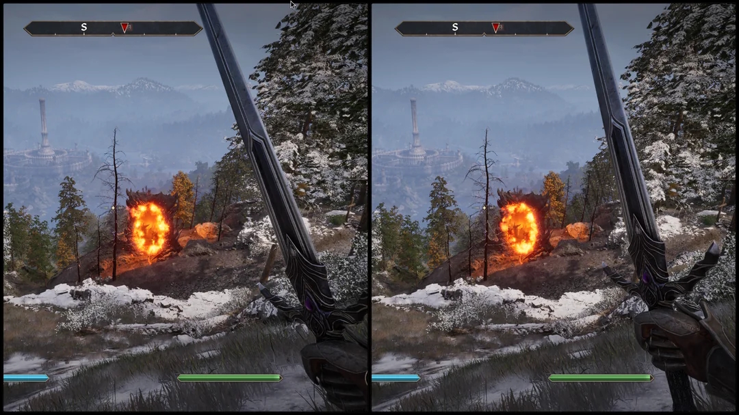
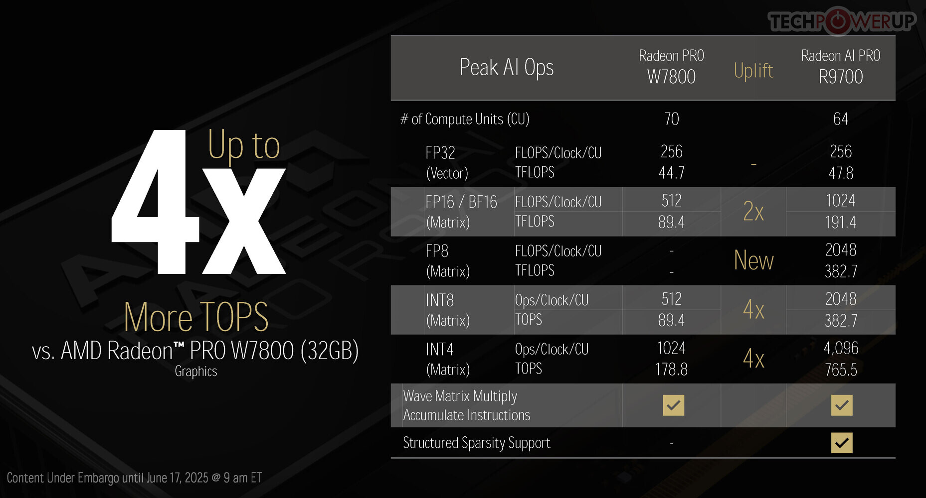
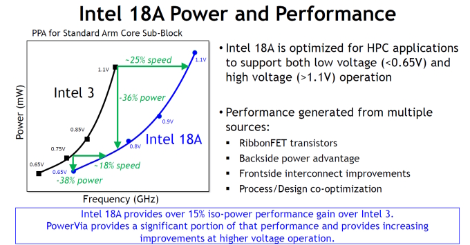
The integration of PowerVia is a game-changer. By routing power through the back of the chip, Intel has managed to tighten the connection pitches on critical front-side layers, while simultaneously relaxing spacing on the very top layers. This strategic shift not only promises to enhance manufacturing yield but also significantly simplifies the fabrication process itself. As shown by HardwareLuxx, the numbers speak volumes: in standardised power, performance, and area (PPA) tests conducted on an Arm core sub-block, Intel 18A showcased approximately 15% better iso-power performance than Intel 3. Pushing the voltage to 1.1V, clock speeds can increase up to 25% without incurring additional energy expenditures. Even at a lower 0.75V, performance can improve by 18%, or power consumption can be slashed by nearly 40%.
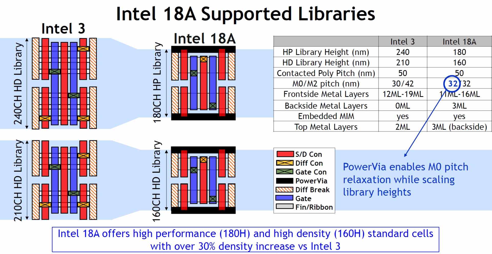
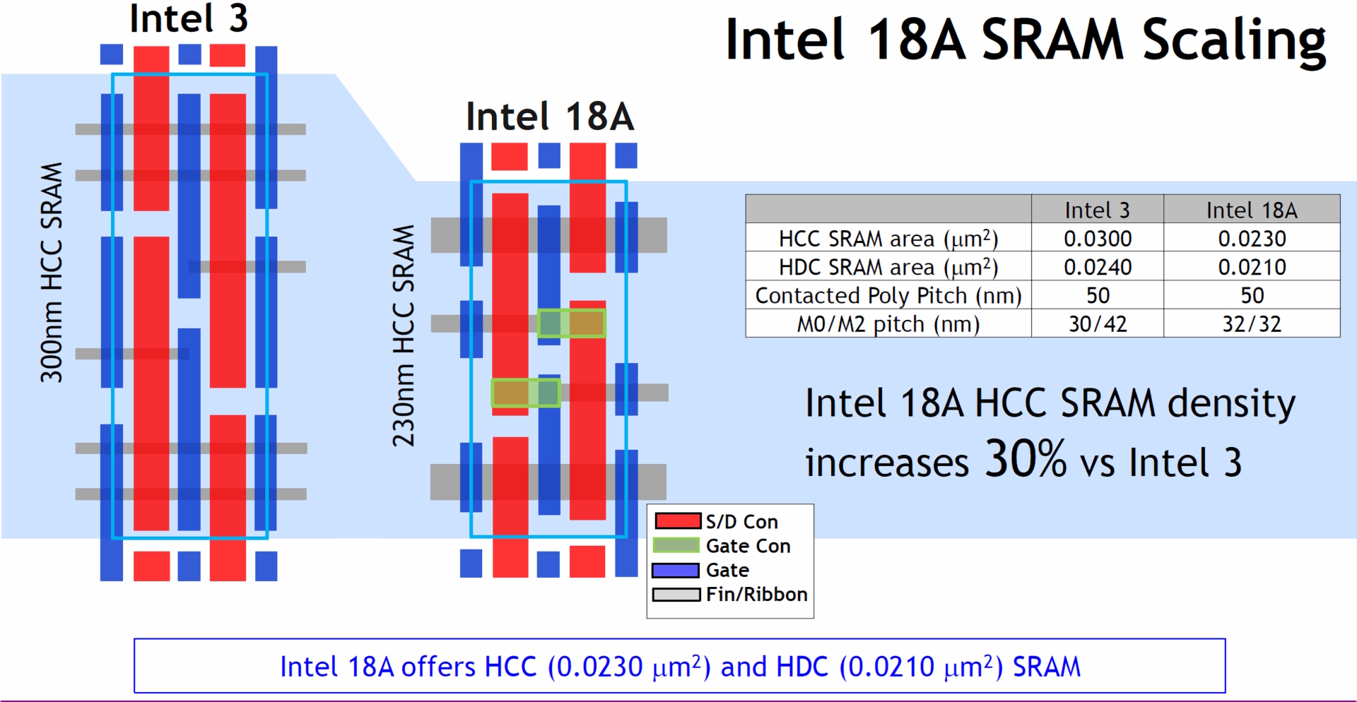
Under the hood, this process node achieves substantial reductions in cell height. Performance-tuned cells now measure a compact 180 nanometres, while high-density designs shrink further to just 160 nm, both notably smaller than their predecessors. The structure of metal layers has also been refined, as the front-side layers have been reduced from a range of 12-19 on Intel 3 to 11-16 on Intel 18A. To facilitate PowerVia, three additional rear metal layers have been added. Moreover, the pitches on the lower metal layers (M1 through M10) have been dramatically tightened, going from as much as 60 nm down to 32 nm, before intentionally increasing again in the uppermost layers. Adding to the manufacturing efficiency, low-NA EUV exposure is employed on layers M0 through M4, which slashes the number of masks required by an impressive 44%, further simplifying the overall production flow.
Intel intends to debut its 18A technology in key upcoming products. This includes the low-power Panther Lake, aimed at mobile platforms, and the efficiency-core-only “Clearwater Forest” Xeon 7 series for server applications. Recognising the diverse needs of different markets, Intel will offer multiple variations of the 18A process, including a cost-optimised 17-layer variant, a balanced 21-layer option, and a performance-focused 22-layer arrangement, ensuring flexibility for a wide range of applications.
KitGuru says: Can Intel recover its footing in the foundry business with its new 18A process node?
The post Intel 18A process node claimed to be 25% faster than previous generation first appeared on KitGuru.