The U.S. reneged on aid commitments. Nepal’s malnourished children are paying the price
Hard-won progress in improving child and maternal nutrition hangs in the balance

IRVINE, Calif. – June 26, 2025 – Terran Orbital Corporation, a leading manufacturer of satellite products for the aerospace and defense industry, is proud to announce the adoption of a […]
The post Terran Orbital Implements Alternative Workweek Schedule to Improve Efficiency and Support Employees appeared first on SpaceNews.

The Pentagon has no backup plan if the massive reconciliation package fails to pass
The post Trump’s ‘One Big, Beautiful Bill’ would give Space Force a nearly $40 billion budget appeared first on SpaceNews.

An agreement between the United States and Sweden brings Firefly Aerospace one step closer to launching its Alpha rocket from a Swedish spaceport.
The post Technology safeguards agreement enables Firefly launches from Sweden appeared first on SpaceNews.
This episode of the Physics World Weekly podcast features Hannah Earley, a mathematician and physicist who is chief technical officer and co-founder of Vaire Computing.
The company is developing hardware for reversible computing, a paradigm with the potential to reduce significantly the energy required to do computations – which could be a boon for power-hungry applications like artificial intelligence.
In a conversation with Physics World’s Margaret Harris, Earley talks about the physics, engineering and commercialization of reversible computing. They also chat about the prototype chips that Vaire is currently working on and the company’s plans for the future.
The post Reversible computing could help solve AI’s looming energy crisis appeared first on Physics World.

In this week’s episode of Space Minds David Ariosto sits down Nathalie Cabrol, Director of the Carl Sagan Center at the SETI Institute who explains why the Red Planet may hold answers about extraterrestrial life as well as our own origins.
The post What Mars can teach us about life appeared first on SpaceNews.


In-flight connectivity (IFC) is fast becoming a major arena for innovation and growth. As airlines seek new ways to differentiate and drive revenue through enhanced passenger experiences, seamless satellite connectivity […]
The post Deep tech is driving the next frontier in in-flight connectivity appeared first on SpaceNews.

NASA’s acting administrator expects to decide on a new “top-level” structure for the agency within weeks, but a Senate-confirmed administrator may not be in place until next year.
The post NASA’s acting leadership planning new agency structure appeared first on SpaceNews.
A new experiment has offered the clearest view yet of how gluons behave inside atomic nuclei. Conducted at the Thomas Jefferson National Accelerator Facility in the US, the study focused on a rare process called photoproduction. This involves high-energy photons interacting with protons confined in nuclei to produce J/psi mesons. The research sheds light on how gluons are distributed in nuclear matter and is a crucial step toward understanding the nature of protons within nuclei.
While gluons are responsible for generating most of the visible mass in the universe, their role inside nuclei remains poorly understood. These massless particles mediate the strong nuclear force, which binds quarks as well as protons and neutrons in nuclei. Gluons carry no electric charge and cannot be directly detected.
The theory that describes gluons is called quantum chromodynamics (QCD) and it is notoriously complex and difficult to test – especially in the dense, strongly interacting environment of a nucleus. That makes precision experiments essential for revealing how matter is held together at the deepest level.
The Jefferson Lab experiment focused on photoproduction, a process in which a high-energy photon strikes a particle and creates something new, in this case, a J/psi meson.
The J/psi comprises a charm quark and its antiquark and is especially useful for studying gluons. Charm quarks are much heavier than those found in ordinary matter and are not present in protons or neutrons. Therefore, they must be created entirely during the interaction, making the J/psi a particularly clean and sensitive probe of gluon behaviour inside nuclei.
Earlier studies had observed this process using free protons. This new experiment extends the approach to protons confined in nuclei to see how that environment affects gluon behaviour. The modification of quarks inside nuclei has been known since the 1980s and is called the EMC effect. However, much less is known about how gluons behave under the same conditions.
“Protons and neutrons do behave differently when they are bound inside nuclei than they do on their own,” says Jackson Pybus, now a postdoctoral fellow at Los Alamos National Laboratory and one of the experiment’s collaborators. “The nuclear physics community is still trying to work out the mechanisms behind the EMC effect. Until now, the distribution of high-momentum gluons in nuclei has remained an unexplored area.”
Pybus and colleagues used Jefferson Lab’s Experimental Hall D, which delivers an intense beam of high-energy photons. This setup had previously been used to study simpler systems, but this was the first time it was applied to heavier nuclei.
“This study looked for events where a photon strikes a proton inside the nucleus to knock it out while producing a J/psi,” Pybus explains. “By measuring the knocked-out proton, the produced J/psi, and the energy of the photon, we can reconstruct the reaction and learn how the gluons were behaving inside the nucleus.” This was done using the GlueX spectrometer.
Significantly, the experiment was accessing the “threshold” region – where the photon has just enough energy to produce a J/psi meson. Near-threshold interactions are particularly valuable because they are highly sensitive to the gluon structure of the target. Creating a heavy charm-anticharm pair requires a large energy transfer so interactions in this region reveal how gluons behave when little momentum is available. This is a regime where theoretical uncertainties in QCD are especially large.
Even more striking were the observations below this threshold. In so-called “sub-threshold” photoproduction, the incoming photon does not carry enough energy to produce the J/psi on its own, so it must draw additional energy from the internal motion of protons or from the nuclear medium itself. This is a well-understood mechanism in principle, but the rate at which it occurred in the experiment came as a surprise.
“Our study was the first to measure J/psi photoproduction from nuclei in the threshold region,” Pybus said. “The data indicate that the J/psi is produced more commonly than expected from protons that are moving with large momentum inside the nucleus, suggesting that these fast-moving protons could experience significant distortion to their internal gluons.”
The sub-threshold results were even harder to explain. “The number of subthreshold J/psi exceeded expectations,” Pybus added. “That raises questions about how the photon is able to pick up so much energy from the nucleus.”
The results suggest that gluons may be modified inside nuclei in ways that are not described by existing models – suggesting a new frontier in nuclear physics.
“This study has given us the first look at this sort of rare phenomenon that can teach us about the gluon inside the nucleus – just enough data to point to unexpected behaviours,” said Pybus. “Now that we know this measurement is possible, and that there are signs of interesting and unexplored phenomena, we’d like to perform a dedicated measurement focused on pinning down the sort of exotic effects we’re just now glimpsing.”
Follow-up experiments, including those planned at the future Electron-Ion Collider, are expected to build on these results. For now, this first glimpse at gluons in nuclei reveals that even decades after QCD’s development, the inner workings of nuclear matter remain only partially illuminated.
The research is described in Physical Review Letters.
The post Photon collisions provide a glimpse of gluons inside nuclei appeared first on Physics World.

The satellite, built by the California-based startup Muon Space, launched March 14 aboard SpaceX's Transporter-13.
The post First ‘FireSat’ satellite delivers thermal images appeared first on SpaceNews.
Modern-day communications rely on both fibre-optic cables and wireless radiofrequency (RF) microwave communications. Reaching higher data transmission capabilities is going to require technologies that can efficiently process and convert both optical and microwave signals in a small and energy-efficient package that’s compatible with existing communication networks.
Microwave photonics (MWP) is one of the frontrunning technologies, as it can perform signal processing tasks within the optical domain. Current MWP approaches, however, are typically power intensive and often require many off-chip devices to achieve the desired device capabilities and functionalities – so are not very scalable. Researchers from Belgium and France have now managed to overcome some of these limitations, reporting their findings in Nature Communications.
“We wanted to demonstrate that photonic chips can be as versatile as electronic chips, and one of the fields where the two overlap is that of microwave photonics,” one of the paper’s lead authors, Wim Bogaerts from Ghent University, tells Physics World.
The researchers have created a photonic engine that processes microwave and optical signals and can convert the signals between the two domains. It is a silicon chip that can generate and detect optical and analogue electrical signals. The chip uses a combination of tuneable lasers (created by using an optical amplifier with on-chip filter circuits), electro-optic modulators and photodetectors, low-loss waveguides and passive components, and a programmable optical filter – which enables the chip to filter signals in both domains.
“We managed to integrate all key functionalities for manipulation of microwave signals and optical signals together on a single silicon chip and use that chip as a programmable engine in different experimental demonstrations,” says Bogaerts.
This setup allowed the researchers to operate the chip as a black-box microwave photonics processor, where the user can process high-frequency RF signals, without being exposed to the internal optical operations (they are hidden).
Optical signals from an external optical fibre are coupled to the chip using a grating coupler and high-speed RF signals are fed into the chip using electro-optic modulators. The RF signal is imprinted into an optical carrier wavelength – which is generated by the on-chip laser – and the signal is then processed on the chip using an optical filter bank. The signal then gets converted back into an RF signal using photodetectors.
All of the signals travelling into and out of the chip can be confined to the RF domain, so the chip doesn’t require any external optical components, unlike many other MWP devices. Moreover, the signals are locally programmed and tuned using thermo-optic phase shifters, enabling users to select any combination of microwave and optical inputs and outputs across the chip.
The researchers used the photonic engine to create multiple systems that showcase its different optical and RF signal processing capabilities and demonstrate a potential pathway towards smaller MWP systems for high-speed wireless communication networks and microwave sensing applications.
As well as being used for simple light-tuning applications, the chip can also perform optical-to-electrical signal conversion, electrical-to-optical signal conversion, microwave frequency doubling, and microwave/optical filtering and equalization. These functions allow it to be used as a transmitter, receiver, optical/microwave filter, frequency converter or a tuneable opto-electronic oscillator.
When asked about the future of the chip, Bogaerts states that “we plan combine this functionality with more general purpose photonic circuits to enable even more functions and applications to help product developers roll out new photonic products as easily as new electronics products”.
Some other potential applications for the chip that have been touted – but not physically tested in this study – include RF instantaneous frequency measuring, radio-over-fibre links, RF phase tuning, optical and RF switching, optical sensing and signal temporal computing. With so many possibilities, this small-scale and low-power chip could become increasingly important as technologies such as communications advance further.
The post Single silicon chip processes optical and microwave signals appeared first on Physics World.

China could launch a mission involving multiple flybys of asteroid Apophis with a swarm of cubesats when the rocky body approaches Earth in 2029.
The post Chinese scientists push for cubesat swarm mission to fly by infamous asteroid Apophis appeared first on SpaceNews.


At issue is the Trump administration’s proposal to cut roughly $130 million from the NRO’s commercial imagery procurement budget for fiscal 2026
The post Satellite imagery firms escalate warnings over budget cuts appeared first on SpaceNews.

Join us for a webinar that takes you deep into the Geospatial intelligence lifecycle—from the capture of data to the advanced analytical tools and how advances in AI and machine learning are transforming it into actionable insights.
The post Webinar: Geospatial Intelligence – New Data to Solutions (replay) appeared first on SpaceNews.


Rocket Lab will launch a pair of European navigation technology demonstration satellites, as Europe again is forced to look outside the continent for launch services.
The post Rocket Lab to launch European navigation tech demo satellites appeared first on SpaceNews.

German launch vehicle startup Isar Aerospace has raised 150 million euros ($174 million) in the form of a convertible bond from an American investor.
The post Isar Aerospace raises 150 million euros appeared first on SpaceNews.

Lux Aeterna has emerged from stealth with $4 million in pre-seed funding to develop a fully reusable satellite slated to launch in 2027, equipped with a heat shield and parachute for safe atmospheric reentry and landing.
The post Lux Aeterna emerges from stealth with funds for fully reusable satellite platform appeared first on SpaceNews.
The development of advance quantum materials and devices often involves making measurements at very low temperatures. This is crucial when developing single-photon emitters and detectors for quantum technologies. And even if a device or material will not be used at cryogenic temperatures, researchers will sometimes make measurements at low temperatures in order to reduce thermal noise.
This R&D will often involve optical techniques such as spectroscopy and imaging, which use lasers and free-space optics. These optical systems must remain in alignment to ensure the quality and repeatability of the measurements. Furthermore, the vibration of optical components must be kept to an absolute minimum because motion will degrade the performance of instrumentation.
Minimizing vibration is usually achieved by doing experiments on optical tables, which are very large, heavy and rigid in order to dampen motion. Therefore, when a cryogenic cooler (cryocooler) is deployed on an optical table it is crucial that it does not introduce unwanted vibrations.
Closed-cycle cryocoolers offer an efficient way to cool samples to temperatures as low as ~2 K to 4 K (−272 °C to −269 °C). Much like a domestic refrigerator or air conditioner, these cryocoolers involve the cyclic compression and expansion of a gas – which is helium in cryogenic systems.
In 2010 Montana Instruments founder Luke Mauritsen, a mechanical engineer and entrepreneur, recognized that the future development of quantum materials and devices would rely on optical cryostats that allow researchers to make optical measurements at very low temperatures and at very low levels of vibration. To make that possible, Mauritsen founded Montana Instruments, which in 2010 launched its first low-vibration cryostats. Based in Bozeman, Montana, the company was acquired by Sweden’s Atlas Copco in 2022 and it continues to develop cryogenic technologies for cutting-edge quantum science and other demanding applications.
Until recently, all of Montana’s low-vibration optical cryostats used Gifford–McMahon (GM) cryocoolers. While these systems provide low temperatures and low vibrations, they are limited in terms of the cooling power that they can deliver. This is because operating GM cryocoolers at higher powers results in greater vibrations.
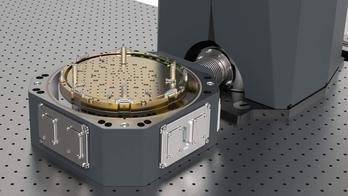
To create a low-vibration cryostat with more cooling power, Montana has developed the Cryostation 200 PT, which is the first Montana system to use a pulse-tube cryocooler. Pulse tubes offer similar cooling powers to GM cryocoolers but at much lower vibration levels. As a result, the Cryostation 200 PT delivers much higher cooling power, while maintaining very low vibrations on par with Montana’s other cryostats.
Montana’s R&D manager Josh Doherty explains, “One major reason that a pulse tube has lower vibrations is that its valve motor can be ‘remote’, located a short distance from coldhead of the cryostat. This allows us to position the valve motor, which generates vibrations, on a cart next to the optical table so its energy can be shunted to the ground, away from the experimental space on the optical table.”
However, isolating the coldhead from the valve motor is not enough to achieve the new cryostat’s very low levels of vibration. During operation, helium gas moves back and forth in the pulse tube and this causes tiny vibrations that are very difficult to mitigate. Using its extensive experience, Montana has minimized the vibrations at the sample/device mount and has also reduced the vibrational energy transferred from the pulse tube to the optical table. Doherty explains that this was done using the company’s patented technologies that minimize the transfer of vibrational energy, while at the same time maximizing thermal conductance between the pulse tube’s first stage and second stage flanges and the sample/device mounting surface(s). This includes the use of flexible, high-thermal-conductivity links and flexible vacuum bellows connections between the coldhead and the sample/device.
Doherty adds, “we intentionally design the supporting structure to de-tune it from the pulse tube vibration source”. This was done by first measuring the pulse-tube vibrations in the lab to determine the vibrational frequencies at which energy is transferred to the optical table. Doherty and colleagues then used the ANSYS engineering/multiphysics software to simulate designs of the pulse tube support and the sample mount supporting structures.
“We optimized the supporting structure design, through material choices, assembly methods and geometry to mismatch the simulated natural frequencies of the support structure from the dominant vibrations of the source,” he explains.
As a result, the Cryostation 200 PT delivers more that 250 mW cooling power at 4.2 K, with a peak-to-peak vibrational amplitude of less than 30 nm. This is more than three times the cooling power delivered by Montana’s Cryostation s200, which offers a similarly-sized sample/device area and vibrational performance.
The control unit has a touchscreen user interface, which displays the cryostat temperature, temperature stability and vacuum pressure.
The cryostat has multiple feedthrough options that support free-space optics, RF and DC electrical connections, optical fibres and a vacuum connection. The Cryostation 200 PT supports Montana’s Cryo-Optic microscope objective and nanopositioner, which can be integrated within the cryostat. Also available is a low working distance window, which supports the use of an external microscope.
According to Montana Instrument senior product manager Patrick Gale, the higher cooling power of the Cryostation 200 PT means that it can support larger experimental payloads – meaning that a much wider range of experiments can be done within the cryostat. For example, more electrical connections can be made with the outside world than had been possible before.
“Every wire that you bring into the cryostat increases that heat load a little bit,” explains Gale, adding, “By using a 1 W pulse tube, we can cool the system down faster than any of our other systems”. While Montana’s other systems have typical cooling times of about 10 h, this has been reduced to about 6 h in the Cryostation 200. “This is particularly important for commercial users who are testing multiple samples in a week,” says Gale. “Saving that four hours per measurement allows a user to do two tests per day, versus just one per day.”
According to Gale, applications of the Cryostation 200 PT include developing ion traps for use in quantum computing, quantum sensing and atomic clocks. Other applications related to quantum technologies include the development of photonic devices; spin-based devices included those based on nitrogen-vacancies in diamond; quantum dots; and superconducting circuits.
The post New optical cryostat combines high cooling capacity, low vibrations and large sample area appeared first on Physics World.