There’s only a few days left in the International Year of Quantum Science and Technology, but we’re still finding plenty to celebrate here at Physics World HQ thanks to a long list of groundbreaking work by quantum physicists in 2025. Here are a few of our favourite stories from the past 12 months.
By this point in 2025, “negative time” may sound like the answer to the question “How long have I got left to buy holiday presents for my loved ones?” Earlier in the year, though, physicists led by experimentalist Aephraim Steinberg of the University of Toronto, Canada and theorist Howard Wiseman of Griffith University in Australia showed that the concept can also describe the average amount of time a photon spends in an excited atomic state. While experts have cautioned against interpreting “negative time” too literally – we aren’t in time machine territory here – it does seem like there’s something interesting going on in this system of ultracold rubidium atoms.
It is a truth universally acknowledged that any sufficiently advanced technology must be in want of a simple system to operate it. In April, the quantum world passed this milestone thanks to Stephanie Wehner and colleagues at Delft University of Technology in the Netherlands. Their operating system is called QNodeOS, and they developed it with the aim of improving access to quantum computing for the 99.99999% percent of people who aren’t (and mostly don’t need to be) intimately familiar with how quantum information processors work. Another advantage of QNodeOS is that it makes it easier for classical and quantum machines (and quantum devices built with different qbit architectures) to communicate with each other.
How big does an object have to be before it stops being quantum and starts behaving like the billiard-ball-like solids familiar from introductory classical mechanics courses? It’s a question that featured in our annual “Breakthrough of the Year” back in 2021, when two independent teams demonstrated quantum entanglement in pairs of 10-micron drumheads, and we’re returning to it this year in a different system: levitated nanoparticles around 100 nm in diameter.
In one boundary-pushing experiment, Massimiliano Rossi and colleagues at ETH Zurich, Switzerland and the Institute of Photonic Sciences in Barcelona, Spain cooled silica nanoparticles enough to extend their wave-like behaviour to 73 pm. In another study, Kiyotaka Aikawa and colleagues at the University of Tokyo, Japan performed the first quantum mechanical squeezing on a nanoparticle, narrowing its velocity distribution at the expense of its momentum distribution. We may not know exactly where the quantum-classical boundary is yet, but the list of quantum behaviours we’ve observed in usually-not-quantum objects keeps getting longer.
What’s the best way to generate random numbers? In part, the answer depends on how random those numbers really need to be. For many applications, the pseudorandom numbers generated by classical computers, or the random-but-with-systematic-biases numbers found in, say, radio static, are good enough. But if you really, really need those numbers to be random, you need a quantum source – and thanks to work published this year by Scott Aaronson, Shi-Han Hung, Marco Pistoia and colleagues, that quantum source can now be a quantum computer. Which is a neat way of tying things together, don’t you think?
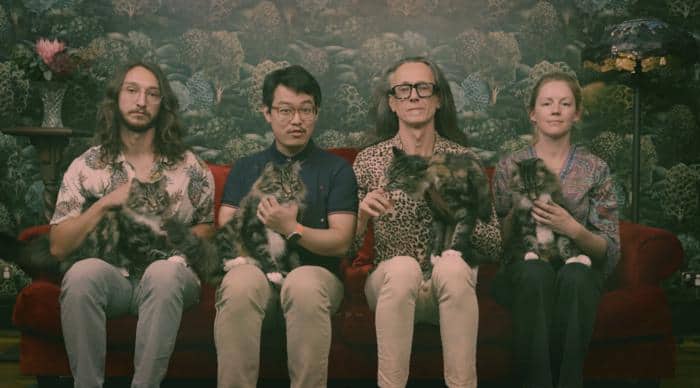
Quantum cats Left to right are UNSW researchers Benjamin Wilhelm, Xi Yu, Andrea Morello, Danielle Holmes. (Courtesy: UNSW Sydney)
Finally, we would be remiss not to mention the work of Andrea Morello and colleagues at the University of New South Wales, Australia. This year, they became the first to create quantum superpositions known as a Schrödinger’s cat states in a heavy atom, antimony, that has a large nuclear spin. They also created what is certainly the year’s best scientific team photo, posing with cats on their laps and deadpan expressions more usually associated with too-cool-for-school indie musicians.
So congratulations to them, and to all the other teams in this list, for setting the bar high in a year that offered plenty for the quantum community to celebrate. We hope you enjoyed the International Year of Quantum Science and Technology, and we look forward to many more exciting discoveries in 2026.
Drinking water in plastic bottles contains countless particles too small to see. New research finds that people who drink water from them on a daily basis ingest far more microplastics than those who don’t.
In the mid-19th century, Bernhard Riemann conceived of a new way to think about mathematical spaces, providing the foundation for modern geometry and physics.
Chinese companies have pledged hundreds of billions of dollars in clean energy manufacturing investments overseas, but the projects are having significant social, environmental, and human rights impacts.
This year saw Physics World report on a raft of innovative and exciting developments in the worlds of medical physics and biotech. These included novel cancer therapies using low-temperature plasma or laser ablation, intriguing new devices such as biodegradable bone screws and a pacemaker smaller than a grain of rice, and neural engineering breakthroughs including an ultrathin bioelectric implant that improves movement in rats with spinal cord injuries and a tiny brain sensor that enables thought control of external devices. Here are a few more research highlights that caught my eye.
Vision transformed
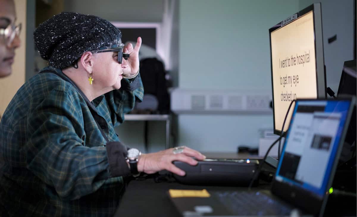
One remarkable device introduced in 2025 was an eye implant that restored vision to patients with incurable sight loss. In a clinical study headed up at the University of Bonn, participants with sight loss due to age-related macular degeneration had a tiny wireless implant inserted under their retina. Used in combination with specialized glasses, the system restored the ability to read in 27 of 32 participants followed up a year later.
Learning to read again Study participant Sheila Irvine, a patient at Moorfields Eye Hospital, training with the PRIMA device. (Courtesy: Moorfields Eye Hospital)
We also described a contact lens that enables wearers to see near-infrared light without night vision goggles, reported on an fascinating retinal stimulation technique that enabled volunteers to see colours never before seen by the human eye, and chatted with researchers in Hungary about how a tiny dissolvable eye insert they are developing could help astronauts suffering from eye conditions.
Radiation therapy advances
2025 saw several firsts in the field of radiation therapy. Researchers in Germany performed the first cancer treatment using a radioactive carbon ion beam, on a mouse with a bone tumour close to the spine. And a team at the Trento Proton Therapy Centre in Italy delivered the first clinical treatments using proton arc therapy – a development that made it onto our top 10 Breakthroughs of the Year.
Meanwhile, the ASTRO meeting saw Leo Cancer Care introduce its first upright photon therapy system, called Grace, which will deliver X-ray radiation to patients in an upright position. This new take on radiation delivery is also under investigation by a team at RaySearch Laboratories, who showed that combining static arcs and shoot-through beams could increase plan quality and reduce delivery times in upright proton therapy.
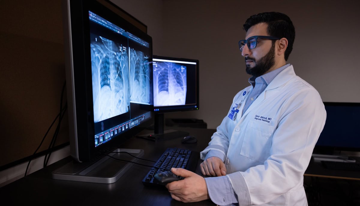
It’s particularly interesting to examine how the rapid evolution of artificial intelligence (AI) is impacting healthcare, especially considering its potential for use in data-intensive tasks. Earlier this year, a team at Northwestern Medicine integrated a generative AI tool into a live clinical workflow for the first time, using it to draft radiology reports on X-ray images. In routine use, the AI model increased documentation efficiency by an average of 15.5%, while maintaining diagnostic accuracy.
Samir Abboud: “For me and my colleagues, it’s not an exaggeration to say that [the AI tool] doubled our efficiency.” (Courtesy: José M Osorio/Northwestern Medicine)
When introducing AI into the clinic, however, it’s essential that any AI-driven software is accurate, safe and trustworthy. To help assess these factors, a multinational research team identified potential pitfalls in the evaluation of algorithmic bias in AI radiology models, suggesting best practices to mitigate such bias.
A quantum focus
Finally, with 2025 being the International Year of Quantum Science and Technology, Physics World examined how quantum physics looks set to play a key role in medicine and healthcare. Many quantum-based companies and institutions are already working in the healthcare sector, with quantum sensors, in particular, close to being commercialized. As detailed in this feature on quantum sensing, such technologies are being applied for applications ranging from lab and point-of-care diagnostics to consumer wearables for medical monitoring, body scanning and microscopy.
Alongside, scientists at Jagiellonian University are applying quantum entanglement to cancer diagnostics and developing the world’s first whole-body quantum PET scanner, while researchers at the University of Warwick have created an ultrasensitive magnetometer based on nitrogen-vacancy centres in diamond that could detect small cancer metastases via keyhole surgery. There’s even a team designing a protein qubit that can be produced directly inside living cells and used as a magnetic field sensor (which also featured in this year’s top 10 breakthroughs).
And in September, we ran a Physics World Live event examining how quantum optics, quantum sensors and quantum entanglement can enable advanced disease diagnostics and transform medical imaging. The recording is available to watch here.
Tory Bruno, who recently stepped down as chief executive of United Launch Alliance, is joining Blue Origin as head of the company’s new national security business unit.
NASA’s Perseverance Mars rover is continuing its mission to collect samples despite uncertainty about how, when or even if those samples will be returned to Earth.
Although wolf-canine interbreeding has been considered extremely rare, the latest research shows that many present-day canines carry a small amount of wolf genes.