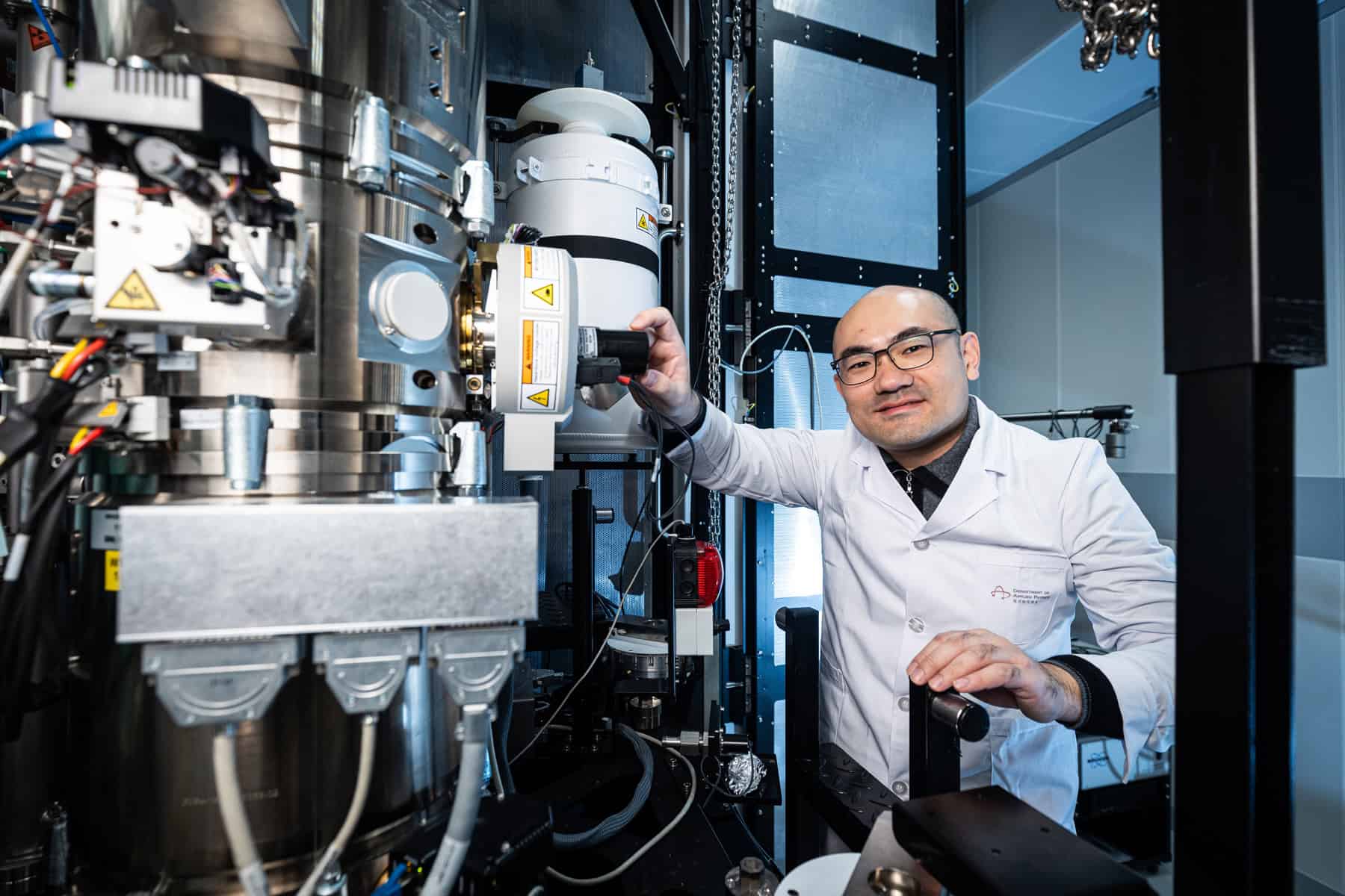
SEMICON Europa 2025 presents cutting-edge technology for semiconductor R&D and production
“Global collaborations for European economic resilience” is the theme of SEMICON Europa 2025. The event is coming to Munich, Germany on 18–21 November and it will attract 25,000 semiconductor professionals who will enjoy presentations from over 200 speakers.
The TechARENA portion of the event will cover a wide range of technology-related issues including new materials, future computing paradigms and the development of hi-tech skills in the European workface. There will also be an Executive Forum, which will feature leaders in industry and government and will cover topics including silicon geopolitics and the use of artificial intelligence in semiconductor manufacturing.
SEMICON Europa will be held at the Messe München, where it will feature a huge exhibition with over 500 exhibitors from around the world. The exhibition is spread out over three halls and here are some of the companies and product innovations to look out for on the show floor.
Accelerating the future of electro-photonic integration with SmarAct
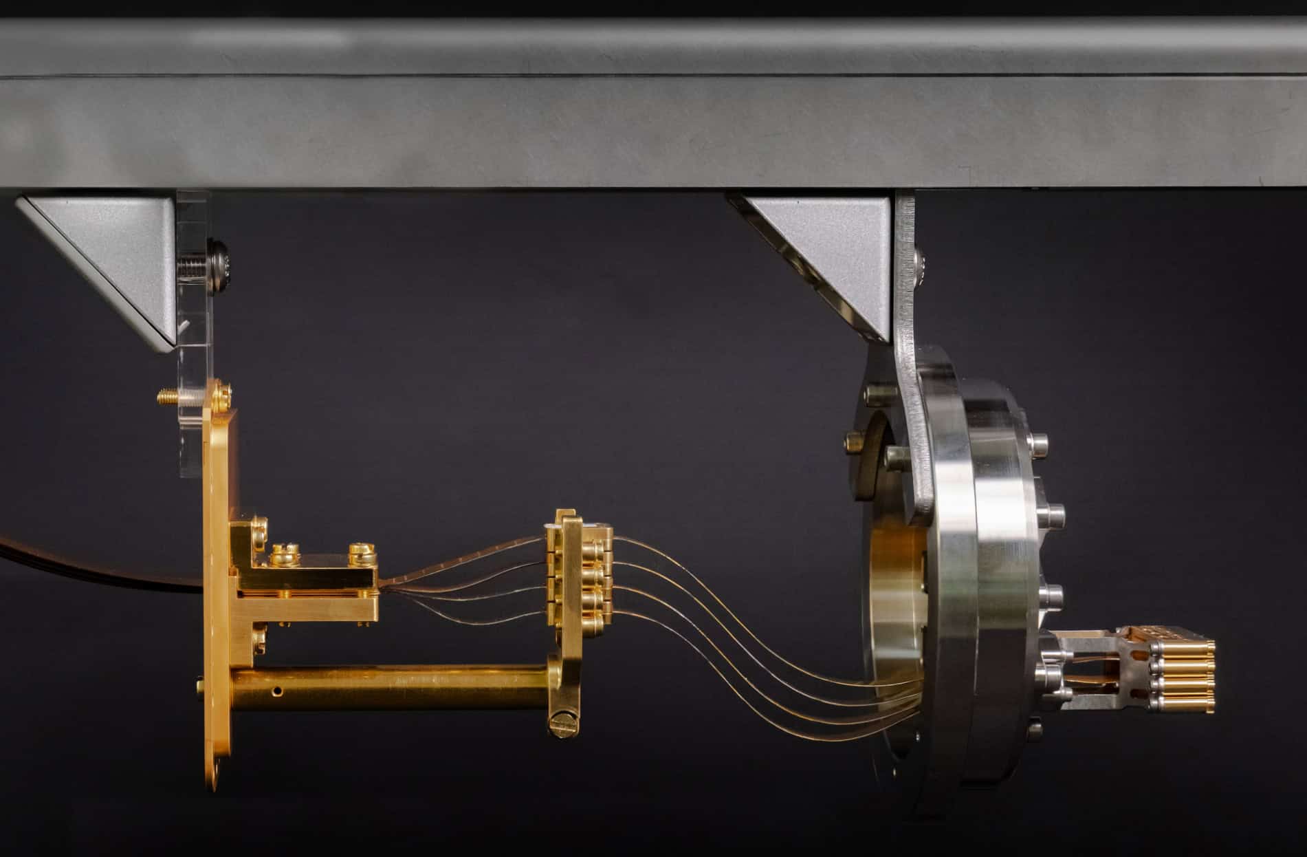
As the boundaries between electronic and photonic technologies continue to blur, the semiconductor industry faces a growing challenge: how to test and align increasingly complex electro-photonic chip architectures efficiently, precisely, and at scale. At SEMICON Europa 2025, SmarAct will address this challenge head-on with its latest innovation – Fast Scan Align. This is a high-speed and high-precision alignment solution that redefines the limits of testing and packaging for integrated photonics.
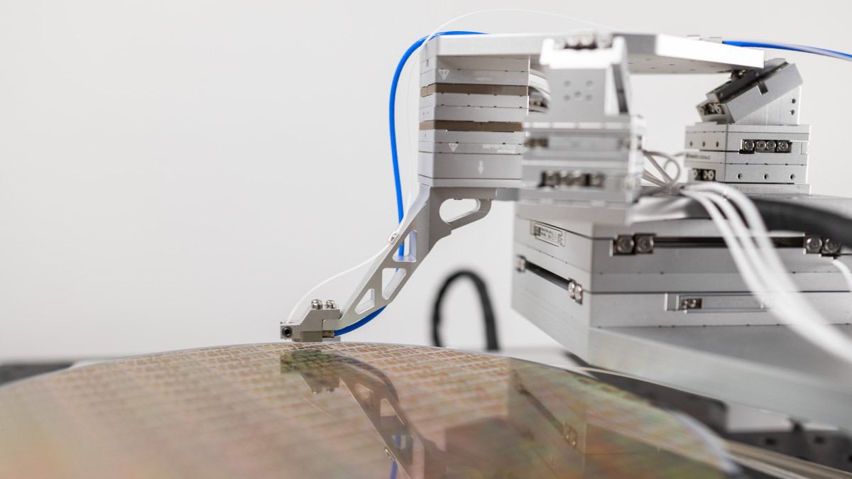
In the emerging era of heterogeneous integration, electronic and photonic components must be aligned and interconnected with sub-micrometre accuracy. Traditional positioning systems often struggle to deliver both speed and precision, especially when dealing with the delicate coupling between optical and electrical domains. SmarAct’s Fast Scan Align solution bridges this gap by combining modular motion platforms, real-time feedback control, and advanced metrology into one integrated system.
At its core, Fast Scan Align leverages SmarAct’s electromagnetic and piezo-driven positioning stages, which are capable of nanometre-resolution motion in multiple degrees of freedom. Fast Scan Align’s modular architecture allows users to configure systems tailored to their application – from wafer-level testing to fibre-to-chip alignment with active optical coupling. Integrated sensors and intelligent algorithms enable scanning and alignment routines that drastically reduce setup time while improving repeatability and process stability.
Fast Scan Align’s compact modules allow various measurement techniques to be integrated with unprecedented possibilities. This has become decisive for the increasing level of integration of complex electro-photonic chips.
Apart from the topics of wafer-level testing and packaging, wafer positioning with extreme precision is as crucial as never before for the highly integrated chips of the future. SmarAct’s PICOSCALE interferometer addresses the challenge of extreme position by delivering picometer-level displacement measurements directly at the point of interest.
When combined with SmarAct’s precision wafer stages, the PICOSCALE interferometer ensures highly accurate motion tracking and closed-loop control during dynamic alignment processes. This synergy between motion and metrology gives users unprecedented insight into the mechanical and optical behaviour of their devices – which is a critical advantage for high-yield testing of photonic and optoelectronic wafers.
Visitors to SEMICON Europa will also experience how all of SmarAct’s products – from motion and metrology components to modular systems and up to turn-key solutions – integrate seamlessly, offering intuitive operation, full automation capability, and compatibility with laboratory and production environments alike.
For more information visit SmarAct at booth B1.860 or explore more of SmarAct’s solutions in the semiconductor and photonics industry.
Optimized pressure monitoring: Efficient workflows with Thyracont’s VD800 digital compact vacuum meters
Thyracont Vacuum Instruments will be showcasing its precision vacuum metrology systems in exhibition hall C1. Made in Germany, the company’s broad portfolio combines diverse measurement technologies – including piezo, Pirani, capacitive, cold cathode, and hot cathode – to deliver reliable results across a pressure range from 2000 to 3e-11 mbar.
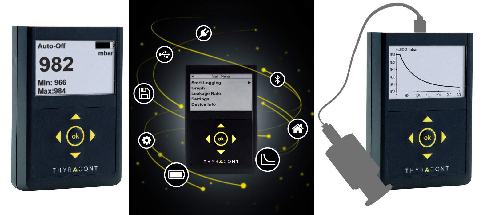
Front-and-centre at SEMICON Europa will be Thyracont’s new series of VD800 compact vacuum meters. These instruments provide precise, on-site pressure monitoring in industrial and research environments. Featuring a direct pressure display and real-time pressure graphs, the VD800 series is ideal for service and maintenance tasks, laboratory applications, and test setups.
The VD800 series combines high accuracy with a highly intuitive user interface. This delivers real-time measurement values; pressure diagrams; and minimum and maximum pressure – all at a glance. The VD800’s 4+1 membrane keypad ensures quick access to all functions. USB-C and optional Bluetooth LE connectivity deliver seamless data readout and export. The VD800’s large internal data logger can store over 10 million measured values with their RTC data, with each measurement series saved as a separate file.
Data sampling rates can be set from 20 ms to 60 s to achieve dynamic pressure tracking or long-term measurements. Leak rates can be measured directly by monitoring the rise in pressure in the vacuum system. Intelligent energy management gives the meters extended battery life and longer operation times. Battery charging is done conveniently via USB-C.
The vacuum meters are available in several different sensor configurations, making them adaptable to a wide range of different uses. Model VD810 integrates a piezo ceramic sensor for making gas-type-independent measurements for rough vacuum applications. This sensor is insensitive to contamination, making it suitable for rough industrial environments. The VD810 measures absolute pressure from 2000 to 1 mbar and relative pressure from −1060 to +1200 mbar.
Model VD850 integrates a piezo/Pirani combination sensor, which delivers high resolution and accuracy in the rough and fine vacuum ranges. Optimized temperature compensation ensures stable measurements in the absolute pressure range from 1200 to 5e-5 mbar and in the relative pressure range from −1060 to +340 mbar.
The model VD800 is a standalone meter designed for use with Thyracont’s USB-C vacuum transducers, which are available in two models. The VSRUSB USB-C transducer is a piezo/Pirani combination sensor that measures absolute pressure in the 2000 to 5.0e-5 mbar range. The other is the VSCUSB USB-C transducer, which measures absolute pressures from 2000 down to 1 mbar and has a relative pressure range from -1060 to +1200 mbar. A USB-C cable connects the transducer to the VD800 for quick and easy data retrieval. The USB-C transducers are ideal for hard-to-reach areas of vacuum systems. The transducers can be activated while a process is running, enabling continuous monitoring and improved service diagnostics.
With its blend of precision, flexibility, and ease of use, the Thyracont VD800 series defines the next generation of compact vacuum meters. The devices’ intuitive interface, extensive data capabilities, and modern connectivity make them an indispensable tool for laboratories, service engineers, and industrial operators alike.
To experience the future of vacuum metrology in Munich, visit Thyracont at SEMICON Europa hall C1, booth 752. There you will discover how the VD800 series can optimize your pressure monitoring workflows.
The post SEMICON Europa 2025 presents cutting-edge technology for semiconductor R&D and production appeared first on Physics World.