This talk shows how integrating p-type NiO to form NiO/Ga₂O₃ heterojunction rectifiers overcomes that barrier, enabling record-class breakdown and Ampere-class operation. It will cover device structure/process optimization, thermal stability to high temperatures, and radiation response – with direct ties to today’s priorities: EV fast charging, AI data‑center power systems, and aerospace/space‑qualified power electronics.
An interactive Q&A session follows the presentation.
Jian-Sian Li
Jian-Sian Li received the PhD in chemical engineering from the University of Florida in 2024, where his research focused on NiO/β-Ga₂O₃ heterojunction power rectifiers, includes device design, process optimization, fast switching, high-temperature stability, and radiation tolerance (γ, neutron, proton). His work includes extensive electrical characterization and microscopy/TCAD analysis supporting device physics and reliability in harsh environments. Previously, he completed his BS and MS at National Taiwan University (2015, 2018), with research spanning phoretic/electrokinetic colloids, polymers for OFETs/PSCs, and solid-state polymer electrolytes for Li-ion batteries. He has since transitioned to industry at Micron Technology.
A new integrated “snapshot spectroscopy” system developed in China can determine the spectral and spatial composition of light from an object with much better precision than other existing systems. The instrument uses randomly textured lithium niobate and its developers have used it for astronomical imaging and materials analysis – and they say that other applications are possible.
Spectroscopy is crucial to analysis of all kinds of objects in science and engineering, from studying the radiation emitted by stars to identifying potential food contaminants. Conventional spectrometers – such as those used on telescopes – rely on diffractive optics to separate incoming light into its constituent wavelengths. This makes them inherently large, expensive and inefficient at rapid image acquisition as the light from each point source has to be spatially separated to resolve the wavelength components.
In recent years researchers have combined computational methods with advanced optical sensors to create computational spectrometers with the potential to rival conventional instruments. One such approach is hyperspectral snapshot imaging, which captures both spectral and spatial information in the same image. There are currently two main snapshot-imaging techniques available. Narrowband-filtered snapshot spectral imagers comprise a mosaic pattern of narrowband filters and acquire an image by taking repeated snapshots at different wavelengths. However, these trade spectral resolution with spatial resolution, as each extra band requires its own tile within the mosaic. A more complex alternative design – the broadband-modulated snapshot spectral imager – uses a single, broadband detector covered with a spatially varying element such as a metasurface that interacts with the light and imprints spectral encoding information onto each pixel. However, these are complex to manufacture and their spectral resolution is limited to the nanometre scale.
Random thicknesses
In the new work, researchers led by Lu Fang at Tsinghua University in Beijing unveil a spectroscopy technique that utilizes the nonlinear optical properties of lithium niobate to achieve sub-Ångström spectral resolution in a simply fabricated, integrated snapshot detector they call RAFAEL. A lithium niobate layer with random, sub-wavelength thickness variations is surrounded by distributed Bragg reflectors, forming optical cavities. These are integrated into a stack with a set of electrodes. Each cavity corresponds to a single pixel. Incident light enters from one side of a cavity, interacting with the lithium niobate repeatedly before exiting and being detected. Because lithium niobate is nonlinear, its response varies with the wavelength of the light.
The researchers then applied a bias voltage using the electrodes. The nonlinear optical response of lithium niobate means that this bias alters its response to light differently at different wavelengths. Moreover, the random variation of the lithium niobate’s thickness around the surface means that the wavelength variation is spatially specific.
The researchers designed a machine learning algorithm and trained it to use this variation of applied bias voltage with resulting wavelength detected at each point to reconstruct the incident wavelengths on the detector at each point in space.
“The randomness is useful for making the equations independent,” explains Fang; “We want to have uncorrelated equations so we can solve them.”
Thousands of stars
The researchers showed that they could achieve 88 Hz snapshot spectroscopy on a grid of 2048×2048 pixels with a spectral resolution of 0.5 Å (0.05 nm) between wavelengths of 400–1000 nm. They demonstrated this by capturing the full atomic absorption spectra of up to 5600 stars in a single snapshot. This is a two to four orders of magnitude improvement in observational efficiency over world-class astronomical spectrometers. They also demonstrated other applications, including a materials analysis challenge involving the distinction of a real leaf from a fake one. The two looked identical at optical wavelengths, but, using its broader range of wavelengths, RAFAEL was able to distinguish between the two.
The researchers are now attempting to improve the device further: “I still think that sub-Ångstrom is not the ending – it’s just the starting point,” says Fu. “We want to push the limit of our resolution to the picometre.” In addition, she says, they are working on further integration of the device – which requires no specialized lithography – for easier use in the field. “We’ve already put this technology on a drone platform,” she reveals. The team is also working with astronomical observatories such as Gran Telescopio Canarias in La Palma, Spain.
Computational imaging expert David Brady of Duke University in North Carolina is impressed by the instrument. “It’s a compact package with extremely high spectral resolution,” he says; “Typically an optical instrument, like a CMOS sensor that’s used here, is going to have between 10,000 and 100,000 photo-electrons per pixel. That’s way too many photons for getting one measurement…I think you’ll see that with spectral imaging as is done here, but also with temporal imaging. People are saying you don’t need to go at 30 frames second, you can go at a million frames per second and push closer to the single photon limit, and then that would require you to do computation to figure out what it all means.”
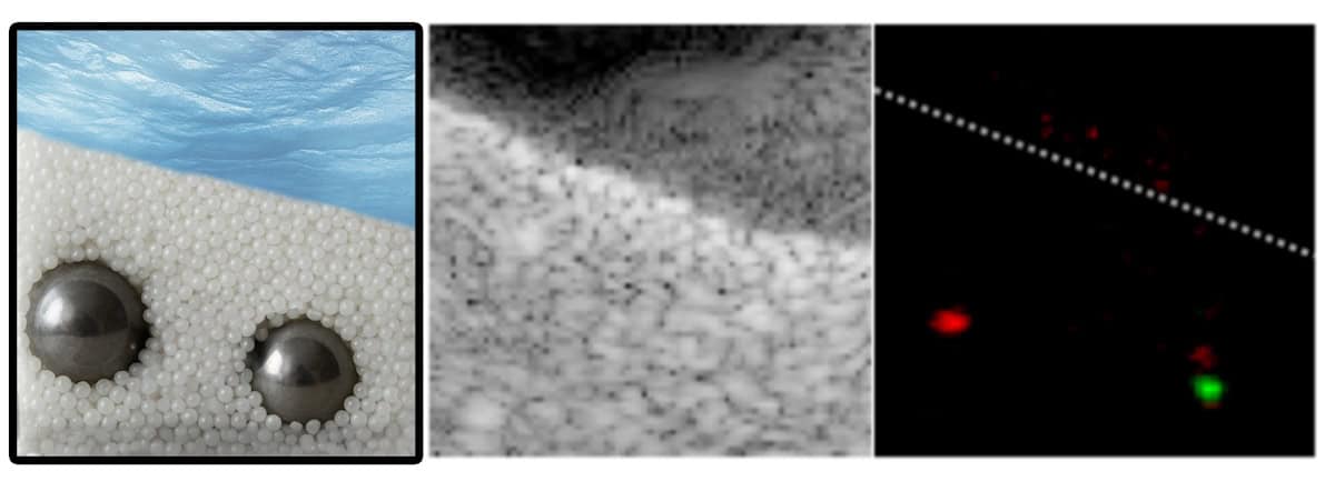
Imaging buried objects Left: artistic impression of metal spheres buried in small glass beads; centre: conventional ultrasound image; right: the new technology can precisely determine the positions of the metal spheres. (Courtesy: TU Wien/Arthur Le Ber)
Physicists have developed a novel imaging technique for detecting and characterizing objects hidden within opaque, highly scattering material. The researchers, from France and Austria, showed that their new mathematical approach, which utilizes the fact that hidden objects generate their own complex scattering pattern, or “fingerprint”, can work on biological tissue.
Viewing the inside of the human body is challenging due to the scattering nature of tissue. With ultrasound, when waves propagate through tissue they are reflected, bounce around and scatter chaotically, creating noise that obscures the signal from the object that the medical practitioner is trying to see. The further you delve into the body the more incoherent the image becomes.
There are techniques for overcoming these issues, but as scattering increases – in more complex media or as you push deeper through tissue – they struggle and unpicking the required signal becomes too complex.
The scientists behind the latest research, from the Institut Langevin in Paris, France and TU Wien in Vienna, Austria, say that rather than compensating for scattering, their technique instead relies on detecting signals from the hidden object in the disorder.
Objects buried in a material create their own complex scattering pattern, and the researchers found that if you know an object’s specific acoustic signal it’s possible to find it in the noise created by the surrounding environment.
“We cannot see the object, but the backscattered ultrasonic wave that hits the microphones of the measuring device still carries information about the fact that it has come into contact with the object we are looking for,” explains Stefan Rotter, a theoretical physicist at TU Wien.
Rotter and his colleagues examined how a series of objects scattered ultrasound waves in an interference-free environment. This created what they refer to as fingerprint matrices: measurements of the specific, characteristic way in which each object scattered the waves.
The team then developed a mathematical method that allowed them to calculate the position of each object when hidden in a scattering medium, based on its fingerprint matrix.
“From the correlations between the measured reflected wave and the unaltered fingerprint matrix, it is possible to deduce where the object is most likely to be located, even if the object is buried,” explains Rotter.
The team tested the technique in three different scenarios. The first experiment trialled the ultrasound imaging of metal spheres in a dense suspension of glass beads in water. Conventional ultrasound failed in this setup and the spheres were completely invisible, but with their novel fingerprint method the researchers were able to accurately detect them.
Next, to examine a medical application for the technique, the researchers embedded lesion markers often used to monitor breast tumours in a foam designed to mimic the ultrasound scattering of soft tissue. These markers can be challenging to detect due to scatterers randomly distributed in human tissue. With the fingerprint matrix, however, the researchers say that the markers were easy to locate.
Finally, the team successfully mapped muscle fibres in a human calf using the technique. They claim this could be useful for diagnosing and monitoring neuromuscular diseases.
According to Rotter and his colleagues, their fingerprint matrix method is a versatile and universal technique that could be applied beyond ultrasound to all fields of wave physics. They highlight radar and sonar as examples of sensing techniques where target identification and detection in noisy environments are long-standing challenges.
“The concept of the fingerprint matrix is very generally applicable – not only for ultrasound, but also for detection with light,” Rotter says. “It opens up important new possibilities in all areas of science where a reflection matrix can be measured.”
The researchers report their findings in Nature Physics.
Radiation treatment for patients with lung cancer represents a balancing act, particularly if malignant lesions are centrally located near to critical structures. The radiation may destroy the tumour, but vital organs may be seriously damaged as well.
The standard treatment for non-small cell lung cancer (NSCLC) is stereotactic ablative body radiotherapy (SABR), which delivers intense radiation doses in just a few treatment sessions and achieves excellent local control. For ultracentral lung legions, however – defined as having a planning target volume (PTV) that abuts or overlaps the proximal bronchial tree, oesophagus or pulmonary vessels – the high risk of severe radiation toxicity makes SABR highly challenging.
A research team at GenesisCare UK, an independent cancer care provider operating nine treatment centres in the UK, has now demonstrated that stereotactic MR-guided adaptive radiotherapy (SMART)-based SABR may be a safer and more effective option for treating ultracentral metastatic lesions in patients with histologically confirmed NSCLC. They report their findings in Advances in Radiation Oncology.
SMART uses diagnostic-quality MR scans to provide real-time imaging, 3D multiplanar soft-tissue tracking and automated beam control of an advanced linear accelerator. The idea is to use daily online volume adaptation and plan re-optimization to account for any changes in tumour size and position relative to organs-at-risk (OAR). Real-time imaging enables treatment in breath-hold with gated beam delivery (automatically pausing delivery if the target moves outside a defined boundary), eliminating the need for an internal target volume and enabling smaller PTV margins.
The approach offers potential to enhance treatment precision and target coverage while improving sparing of adjacent organs compared with conventional SABR, first author Elena Moreno-Olmedo and colleagues contend.
A safer treatment option
The team conducted a study to assess the incidence of SABR-related toxicities in patients with histologically confirmed NSCLC undergoing SMART-based SABR. The study included 11 patients with 18 ultracentral lesions, the majority of whom had oligometastatic or olioprogressive disease.
Patients received five to eight treatment fractions, to a median dose of 40 Gy (ranging from 30 to 60 Gy). The researchers generated fixed-field SABR plans with dosimetric aims including a PTV V100% (the volume receiving at least 100% of the prescription dose) of 95% or above, a PTV V95% of 98% or above and a maximum dose of between110% and 140%. PTV coverage was compromised where necessary to meet OAR constraints, with a minimum PTV V100% of at least 70%.
SABR was performed using a 6 MV 0.35 T MRIdian linac with gated delivery during repeated breath-holds, under continuous MR guidance. Based on daily MRI scans, online plan adaptation was performed for all of the 78 delivered fractions.
The researchers report that both the PTV volume and PTV overlap with ultracentral OARs were reduced in SMART treatments compared with conventional SABR. The median SMART PTV was 10.1 cc, compared with 30.4 cc for the simulated SABR PTV, while the median PTV overlap with OARs was 0.85 cc for SMART (8.4% of the PTV) and 4.7 cc for conventional SABR.
In terms of treatment-related side effects for SMART, the rates of acute and late grade 1–2 toxicities were 54% and 18%, respectively, with no grade 3–5 toxicities observed. This demonstrates the technique’s increased safety compared with non-adaptive SABR treatments, which have exhibited severe rates of toxicity, including treatment-related deaths, in ultracentral tumours.
Two-thirds of patients were alive at the median follow-up point of 28 months, and 93% were free from local progression at 12 months. The median progression-free survival was 5.8 months and median overall survival was 20 months.
Acknowledging the short follow-up time frame, the researchers note that additional late toxicities may occur. However, they are hopeful that SMART will be considered as a favourable treatment option for patients with ultracentral NSCLC lesions.
“Our analysis demonstrates that hypofractionated SMART with daily online adaptation for ultracentral NSCLC achieved comparable local control to conventional non-adaptive SABR, with a safer toxicity profile,” they write. “These findings support the consideration of SMART as a safer and effective treatment option for this challenging subgroup of thoracic tumours.”
The SUNSET trial
SMART-based SABR radiotherapy remains an emerging cancer treatment that’s not available yet in many cancer treatment centres. Despite the high risk for patients with ultracentral tumours, SABR is the standard treatment for inoperable NSCLC.
The phase 1 clinical trial, Stereotactic radiation therapy for ultracentral NSCLC: a safety and efficacy trial (SUNSET), assessed the use of SBRT for ultracentral tumours in 30 patients with early-stage NSCLC treated at five Canadian cancer centres. In all cases, the PTVs touched or overlapped the proximal bronchial tree, the pulmonary artery, the pulmonary vein or the oesophagus. Led by Meredith Giuliani of the Princess Margaret Cancer Centre, the trial aimed to determine the maximum tolerated radiation dose associated with a less than 30% rate of grade 3–5 toxicity within two years of treatment.
All patients received 60 Gy in eight fractions. Dose was prescribed to deliver a PTV V100% of 95%, a PTV V90% of 99% and a maximum dose of no more than 120% of the prescription dose, with OAR constraints prioritized over PTV coverage. All patients had daily cone-beam CT imaging to verify tumour position before treatment.
At a median follow-up of 37 months, two patients (6.7%) experienced dose-limiting grade 3–5 toxicities – an adverse event rate within the prespecified acceptability criteria. The three-year overall survival was 72.5% and the three-year progression-free survival was 66.1%.
In a subsequent dosimetric analysis, the researchers report that they did not identify any relationship between OAR dose and toxicity, within the dose constraints used in the SUNSET trial. They note that 73% of patients could be treated without compromise of the PTV, and where compromise was needed, the mean PTV D95 (the minimum dose delivered to 95% of the PTV) remained high at 52.3 Gy.
As expected, plans that overlapped with central OARs were associated with worse local control, but PTV undercoverage was not. “[These findings suggest] that the approach of reducing PTV coverage to meet OAR constraints does not appear to compromise local control, and that acceptable toxicity rates are achievable using 60 Gy in eight fractions,” the team writes. “In the future, use of MRI or online adaptive SBRT may allow for safer treatment delivery by limiting dose variation with anatomic changes.”
Researchers in the United Arab Emirates have designed a new catheter that can deliver drugs to entire regions of the brain. Developed by Batoul Khlaifat and colleagues at New York University Abu Dhabi, the catheter’s helical structure and multiple outflow ports could make it both safer and more effective for treating a wide range of neurological disorders.
Modern treatments for brain-related conditions including Parkinson’s disease, epilepsy, and tumours often involve implanting microfluidic catheters that deliver controlled doses of drug-infused fluids to highly localized regions of the brain. Today, these implants are made from highly flexible materials that closely mimic the soft tissue of the brain. This makes them far less invasive than previous designs.
However, there is still much room for improvement, as Khlaifat explains. “Catheter design and function have long been limited by the neuroinflammatory response after implantation, as well as the unequal drug distribution across the catheter’s outlets,” she says.
A key challenge with this approach is that each of the brain’s distinct regions has highly irregular shapes, which makes it incredibly difficult to target via single drug doses. Instead, doses must be delivered either through repeated insertions from a single port at the end of a catheter, or through single insertions across multiple co-implanted catheters. Either way, the approach is highly invasive, and runs the risk of further trauma to the brain.
Multiple ports
In their study, Khlaifat’s team explored how many of these problems stem from existing catheter designs. They tend to be simple tubes with single input and output ports at either end. Using fluid dynamics simulations, they started by investigating how drug outflow would change when multiple output ports are positioned along the length of the catheter.
To ensure this outflow is delivered evenly, they carefully adjusted the diameter of each port to account for the change in fluid pressure along the catheter’s length – so that four evenly spaced ports could each deliver roughly one quarter of the total flow. Building on this innovation, the researchers then explored how the shape of the catheter itself could be adjusted to optimize delivery even further.
“We varied the catheter design from a straight catheter to a helix of the same small diameter, allowing for a larger area of drug distribution in the target implantation region with minimal invasiveness,” explains team member Khalil Ramadi. “This helical shape also allows us to resist buckling on insertion, which is a major problem for miniaturized straight catheters.”
Helical catheter
Based on their simulations, the team fabricated a helical catheter the call Strategic Precision Infusion for Regional Administration of Liquid, or SPIRAL. In their first set of experiments, they tested their simulations in controlled lab conditions. They verified their prediction of even outflow rates across the catheter’s outlets.
“Our helical device was also tested in mouse models alongside its straight counterpart to study its neuroinflammatory response,” Khlaifat says. “There were no significant differences between the two designs.”
Having validated the safety of their approach, the researchers are now hopeful that SPIRAL could pave the way for new and improved methods for targeted drug delivery within the brain. With the ability to target entire regions of the brain with smaller, more controlled doses, this future generation of implanted catheters could ultimately prove to be both safer and more effective than existing designs.
“These catheters could be optimized for each patient through our computational framework to ensure only regions that require dosing are exposed to therapy, all through a single insertion point in the skull,” describes team member Mahmoud Elbeh. “This tailored approach could improve therapies for brain disorders such as epilepsy and glioblastomas.”
Quantum connections Measurement scientists are seeking to understand and quantify the relative performance of quantum computers from different manufacturers as well as across the myriad platform technologies. (Courtesy: iStock/Bartlomiej Wroblewski)
From quantum utility today to quantum advantage tomorrow: incumbent technology companies – among them Google, Amazon, IBM and Microsoft – and a wave of ambitious start-ups are on a mission to transform quantum computing from applied research endeavour to mainstream commercial opportunity. The end-game: quantum computers that can be deployed at-scale to perform computations significantly faster than classical machines while addressing scientific, industrial and commercial problems beyond the reach of today’s high-performance computing systems.
Meanwhile, as technology translation gathers pace across the quantum supply chain, government laboratories and academic scientists must maintain their focus on the “hard yards” of precompetitive research. That means prioritizing foundational quantum hardware and software technologies, underpinned by theoretical understanding, experimental systems, device design and fabrication – and pushing out along all these R&D pathways simultaneously.
Bringing order to disorder
Equally important is the requirement to understand and quantify the relative performance of quantum computers from different manufacturers as well as across the myriad platform technologies – among them superconducting circuits, trapped ions, neutral atoms as well as photonic and semiconductor processors. A case study in this regard is a broad-scope UK research collaboration that, for the past four years, has been reviewing, collecting and organizing a holistic taxonomy of metrics and benchmarks to evaluate the performance of quantum computers against their classical counterparts as well as the relative performance of competing quantum platforms.
Funded by the National Quantum Computing Centre (NQCC), which is part of the UK National Quantum Technologies Programme (NQTP), and led by scientists at the National Physical Laboratory (NPL), the UK’s National Metrology Institute, the cross-disciplinary consortium has taken on an endeavour that is as sprawling as it is complex. The challenge lies in the diversity of quantum hardware platforms in the mix; also the emergence of two different approaches to quantum computing – one being a gate-based framework for universal quantum computation, the other an analogue approach tailored to outperforming classical computers on specific tasks.
“Given the ambition of this undertaking, we tapped into a deep pool of specialist domain knowledge and expertise provided by university colleagues at Edinburgh, Durham, Warwick and several other centres-of-excellence in quantum,” explains Ivan Rungger, a principal scientist at NPL, professor in computer science at Royal Holloway, University of London, and lead scientist on the quantum benchmarking project. That core group consulted widely within the research community and with quantum technology companies across the nascent supply chain. “The resulting study,” adds Rungger, “positions transparent and objective benchmarking as a critical enabler for trust, comparability and commercial adoption of quantum technologies, aligning closely with NPL’s mission in quantum metrology and standards.”
Not all metrics are equal – or mature
Made to measure NPL’s Institute for Quantum Standards and Technology (above) is the UK’s national metrology institute for quantum science. (Courtesy: NPL)
For context, a number of performance metrics used to benchmark classical computers can also be applied directly to quantum computers, such as the speed of operations, the number of processing units, as well as the probability of errors to occur in the computation. That only goes so far, though, with all manner of dedicated metrics emerging in the past decade to benchmark the performance of quantum computers – ranging from their individual hardware components to entire applications.
Complexity reigns, it seems, and navigating the extensive literature can prove overwhelming, while the levels of maturity for different metrics varies significantly. Objective comparisons aren’t straightforward either – not least because variations of the same metric are commonly deployed; also the data disclosed together with a reported metric value is often not sufficient to reproduce the results.
“Many of the approaches provide similar overall qualitative performance values,” Rungger notes, “but the divergence in the technical implementation makes quantitative comparisons difficult and, by extension, slows progress of the field towards quantum advantage.”
The task then is to rationalize the metrics used to evaluate the performance for a given quantum hardware platform to a minimal yet representative set agreed across manufacturers, algorithm developers and end-users. These benchmarks also need to follow some agreed common approaches to fairly and objectively evaluate quantum computers from different equipment vendors.
With these objectives in mind, Rungger and colleagues conducted a deep-dive review that has yielded a comprehensive collection of metrics and benchmarks to allow holistic comparisons of quantum computers, assessing the quality of hardware components all the way to system-level performance and application-level metrics.
Drill down further and there’s a consistent format for each metric that includes its definition, a description of the methodology, the main assumptions and limitations, and a linked open-source software package implementing the methodology. The software transparently demonstrates the methodology and can also be used in practical, reproducible evaluations of all metrics.
“As research on metrics and benchmarks progresses, our collection of metrics and the associated software for performance evaluation are expected to evolve,” says Rungger. “Ultimately, the repository we have put together will provide a ‘living’ online resource, updated at regular intervals to account for community-driven developments in the field.”
From benchmarking to standards
Innovation being what it is, those developments are well under way. For starters, the importance of objective and relevant performance benchmarks for quantum computers has led several international standards bodies to initiate work on specific areas that are ready for standardization – work that, in turn, will give manufacturers, end-users and investors an informed evaluation of the performance of a range of quantum computing components, subsystems and full-stack platforms.
What’s evident is that the UK’s voice on metrics and benchmarking is already informing the collective conversation around standards development. “The quantum computing community and international standardization bodies are adopting a number of concepts from our approach to benchmarking standards,” notes Deep Lall, a quantum scientist in Rungger’s team at NPL and lead author of the study. “I was invited to present our work to a number of international standardization meetings and scientific workshops, opening up widespread international engagement with our research and discussions with colleagues across the benchmarking community.”
He continues: “We want the UK effort on benchmarking and metrics to shape the broader international effort. The hope is that the collection of metrics we have pulled together, along with the associated open-source software provided to evaluate them, will guide the development of standardized benchmarks for quantum computers and speed up the progress of the field towards practical quantum advantage.”
That’s a view echoed – and amplified – by Cyrus Larijani, NPL’s head of quantum programme. “As we move into the next phase of NPL’s quantum strategy, the importance of evidence-based decision making becomes ever-more critical,” he concludes. “By grounding our strategic choices in robust measurement science and real-world data, we ensure that our innovations not only push the boundaries of quantum technology but also deliver meaningful impact across industry and society.”
Further reading
Deep Lall et al. 2025 A review and collection of metrics and benchmarks for quantum computers: definitions, methodologies and software https://arxiv.org/abs/2502.06717
The headline take from NQCC
Quantum computing technology has reached the stage where a number of methods for performance characterization are backed by a large body of real-world implementation and use, as well as by theoretical proofs. These mature benchmarking methods will benefit from commonly agreed-upon approaches that are the only way to fairly, unambiguously and objectively benchmark quantum computers from different manufacturers.
“Performance benchmarks are a fundamental enabler of technology innovation in quantum computing,” explains Konstantinos Georgopoulos, who heads up the NQCC’s quantum applications team and is responsible for the centre’s liaison with the NPL benchmarking consortium. “How do we understand performance? How do we compare capabilities? And, of course, what are the metrics that help us to do that? These are the leading questions we addressed through the course of this study.
”If the importance of benchmarking is a given, so too is collaboration and the need to bring research and industry stakeholders together from across the quantum ecosystem. “I think that’s what we achieved here,” says Georgopoulos. “The long list of institutions and experts who contributed their perspectives on quantum computing was crucial to the success of this project. What we’ve ended up with are better metrics, better benchmarks, and a better collective understanding to push forward with technology translation that aligns with end-user requirements across diverse industry settings.”
Professor Zhao Jiong, who leads a Master’s programme in microelectronics technology and material, has been recognized for his pioneering research in 2d ferroelectronics (Courtesy: PolyU)
The microelectronics sector is known for its relentless drive for innovation, continually delivering performance and efficiency gains within ever more compact form factors. Anyone aspiring to build a career in this fast-moving field needs not just a thorough grounding in current tools and techniques, but also an understanding of the next-generation materials and structures that will propel future progress.
That’s the premise behind a Master’s programme in microelectronics technology and materials at the Hong Kong Polytechnic University (PolyU). Delivered by the Department for Applied Physics, globally recognized for its pioneering research in technologies such as two-dimensional materials, nanoelectronics and artificial intelligence, the aim is to provide students with both the fundamental knowledge and practical skills they need to kickstart their professional future – whether they choose to pursue further research or to find a job in industry.
“The programme provides students with all the key skills they need to work in microelectronics, such as circuit design, materials processing and failure analysis,” says programme leader Professor Zhao Jiong, who research focuses on 2D ferroelectrics. “But they also have direct access to more than 20 faculty members who are actively investigating novel materials and structures that go beyond silicon-based technologies.”
The course in also unusual in providing a combined focus on electronics engineering and materials science, providing students with a thorough understanding of the underlying semiconductors and device structures as well as their use in mass-produced integrated circuits. That fundamental knowledge is reinforced through regular experimental work, providing the students with hands-on experience of fabricating and testing electronic devices. “Our cleanroom laboratory is equipped with many different instruments for microfabrication, including thin-film deposition, etching and photolithography, as well as advanced characterization tools for understanding their operating mechanisms and evaluating their performance,” adds Zhao.
In a module focusing on thin-film materials, for example, students gain valuable experience from practical sessions that enable them to operate the equipment for different growth techniques, such as sputtering, molecular beam epitaxy, and both physical and chemical vapour deposition. In another module on materials analysis and characterization, the students are tasked with analysing the layered structure of a standard computer chip by making cross-sections that can be studied with a scanning electron microscope.
During the programme students have access to a cleanroom laboratory that gives them hand-on experience of using advanced tools for fabricating and characterizing electronic materials and structures (Courtesy: PolyU)
That practical experience extends to circuit design, with students learning how to use state-of-the-art software tools for configuring, simulating and analysing complex electronic layouts. “Through this experimental work students gain the technical skills they need to design and fabricate integrated circuits, and to optimize their performance and reliability through techniques like failure analysis,” says Professor Dai Jiyan, PolyU Associate Dean of Students, who also teaches the module on thin-film materials. “This hands-on experience helps to prepare them for working in a manufacturing facility or for continuing their studies at the PhD level.”
Also integrated into the teaching programme is the use of artificial intelligence to assist key tasks, such as defect analysis, materials selection and image processing. Indeed, PolyU has established a joint laboratory with Huawei to investigate possible applications of AI tools in electronic design, providing the students with early exposure to emerging computational methods that are likely to shape the future of the microelectronics industry. “One of our key characteristics is that we embed AI into our teaching and laboratory work,” says Dai. “Two of the modules are directly related to AI, while the joint lab with Huawei helps students to experiment with using AI in circuit design.”
Now in its third year, the Master’s programme was designed in collaboration with Hong Kong’s Applied Science and Technology Research Institute (ASTRI), established in 2000 to enhance the competitiveness of the region through the use of advanced technologies. Researchers at PolyU already pursue joint projects with ASTRI in areas like chip design, microfabrication and failure analysis. As part of the programme, these collaborators are often invited to give guest lectures or to guide the laboratory work. “Sometimes they even provide some specialized instruments for the students to use in their experiments,” says Zhao. “We really benefit from this collaboration.”
Once primed with the knowledge and experience from the taught modules, the students have the opportunity to work alongside one of the faculty members on a short research project. They can choose whether to focus on a topic that is relevant to present-day manufacturing, such as materials processing or advanced packaging technologies, or to explore the potential of emerging materials and devices across applications ranging from solar cells and microfluidics to next-generation memories and neuromorphic computing.
“It’s very interesting for the students to get involved in these projects,” says Zhao. “They learn more about the research process, which can make them more confident to take their studies to the next level. All of our faculty members are engaged in important work, and we can guide the students towards a future research field if that’s what they are interested in.”
There are also plenty of progression opportunities for those who are more interested in pursuing a career in industry. As well as providing support and advice through its joint lab in AI, Huawei arranges visits to its manufacturing facilities and offers some internships to interested students. PolyU also organizes visits to Hong Kong’s Science Park, home to multinational companies such as Infineon as well as a large number of start-up companies in the microelectronics sector. Some of these might support a student’s research project, or offer an internship in areas such as circuit design or microfabrication.
The international outlook offered by PolyU has made the Master’s programme particularly appealing to students from mainland China, but Zhao and Dai believe that the forward-looking ethos of the course should make it an appealing option for graduates across Asia and beyond. “Through the programme, the students gain knowledge about all aspects of the microelectronics industry, and how it is likely to evolve in the future,” says Dai. “The knowledge and technical skills gained by the students offer them a competitive edge for building their future career, whether they want to find a job in industry or to continue their research studies.”
NASA’s Jet Propulsion Laboratory (JPL) is to lay off some 550 employees as part of a restructuring that began in July. The action affects about 11% of JPL’s employees and represents the lab’s third downsizing in the past 20 months. When the layoffs are complete by the end of the year, the lab will have roughly 4500 employees, down from about 6500 at the start of 2024. A further 4000 employees have already left NASA during the past six months via sacking, retirement or voluntary buyouts.
Managed by the California Institute of Technology in Pasadena, JPL oversees scientific missions such as the Psyche asteroid probe, the Europa Clipper and the Perseverance rover on Mars. The lab also operates the Deep Space Network that keeps Earth in communication with unmanned space missions. JPL bosses already laid off about 530 staff – and 140 contractors – in February last year followed by another 325 people in November 2024.
JPL director Dave Gallagher insists, however, that the new layoffs are not related to the current US government shutdown that began on 1 October. “[They are] essential to securing JPL’s future by creating a leaner infrastructure, focusing on our core technical capabilities, maintaining fiscal discipline, and positioning us to compete in the evolving space ecosystem,” he says in a message to employees.
Judy Chu, Democratic Congresswoman for the constituency that includes JPL, is less optimistic. “Every layoff devastates the highly skilled and uniquely talented workforce that has made these accomplishments possible,” she says. “Together with last year’s layoffs, this will result in an untold loss of scientific knowledge and expertise that threatens the very future of American leadership in space exploration and scientific discovery.”
John Logsdon, professor emeritus at George Washington University and founder of the university’s Space Policy Institute, says that the cuts are a direct result of the Trump administration’s approach to science and technology. “The administration gives low priority to robotic science and exploration, and has made draconic cuts to the science budget; that budget supports JPL’s work,” he told Physics World. “With these cuts, there is not enough money to support a JPL workforce sized for more ambitious activities. Ergo, staff cuts.”