This talk shows how integrating p-type NiO to form NiO/Ga₂O₃ heterojunction rectifiers overcomes that barrier, enabling record-class breakdown and Ampere-class operation. It will cover device structure/process optimization, thermal stability to high temperatures, and radiation response – with direct ties to today’s priorities: EV fast charging, AI data‑center power systems, and aerospace/space‑qualified power electronics.
An interactive Q&A session follows the presentation.
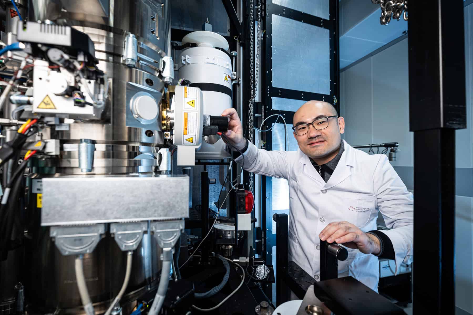
Jian-Sian Li
Jian-Sian Li received the PhD in chemical engineering from the University of Florida in 2024, where his research focused on NiO/β-Ga₂O₃ heterojunction power rectifiers, includes device design, process optimization, fast switching, high-temperature stability, and radiation tolerance (γ, neutron, proton). His work includes extensive electrical characterization and microscopy/TCAD analysis supporting device physics and reliability in harsh environments. Previously, he completed his BS and MS at National Taiwan University (2015, 2018), with research spanning phoretic/electrokinetic colloids, polymers for OFETs/PSCs, and solid-state polymer electrolytes for Li-ion batteries. He has since transitioned to industry at Micron Technology.
Quantum connections Measurement scientists are seeking to understand and quantify the relative performance of quantum computers from different manufacturers as well as across the myriad platform technologies. (Courtesy: iStock/Bartlomiej Wroblewski)
From quantum utility today to quantum advantage tomorrow: incumbent technology companies – among them Google, Amazon, IBM and Microsoft – and a wave of ambitious start-ups are on a mission to transform quantum computing from applied research endeavour to mainstream commercial opportunity. The end-game: quantum computers that can be deployed at-scale to perform computations significantly faster than classical machines while addressing scientific, industrial and commercial problems beyond the reach of today’s high-performance computing systems.
Meanwhile, as technology translation gathers pace across the quantum supply chain, government laboratories and academic scientists must maintain their focus on the “hard yards” of precompetitive research. That means prioritizing foundational quantum hardware and software technologies, underpinned by theoretical understanding, experimental systems, device design and fabrication – and pushing out along all these R&D pathways simultaneously.
Bringing order to disorder
Equally important is the requirement to understand and quantify the relative performance of quantum computers from different manufacturers as well as across the myriad platform technologies – among them superconducting circuits, trapped ions, neutral atoms as well as photonic and semiconductor processors. A case study in this regard is a broad-scope UK research collaboration that, for the past four years, has been reviewing, collecting and organizing a holistic taxonomy of metrics and benchmarks to evaluate the performance of quantum computers against their classical counterparts as well as the relative performance of competing quantum platforms.
Funded by the National Quantum Computing Centre (NQCC), which is part of the UK National Quantum Technologies Programme (NQTP), and led by scientists at the National Physical Laboratory (NPL), the UK’s National Metrology Institute, the cross-disciplinary consortium has taken on an endeavour that is as sprawling as it is complex. The challenge lies in the diversity of quantum hardware platforms in the mix; also the emergence of two different approaches to quantum computing – one being a gate-based framework for universal quantum computation, the other an analogue approach tailored to outperforming classical computers on specific tasks.
“Given the ambition of this undertaking, we tapped into a deep pool of specialist domain knowledge and expertise provided by university colleagues at Edinburgh, Durham, Warwick and several other centres-of-excellence in quantum,” explains Ivan Rungger, a principal scientist at NPL, professor in computer science at Royal Holloway, University of London, and lead scientist on the quantum benchmarking project. That core group consulted widely within the research community and with quantum technology companies across the nascent supply chain. “The resulting study,” adds Rungger, “positions transparent and objective benchmarking as a critical enabler for trust, comparability and commercial adoption of quantum technologies, aligning closely with NPL’s mission in quantum metrology and standards.”
Not all metrics are equal – or mature
Made to measure NPL’s Institute for Quantum Standards and Technology (above) is the UK’s national metrology institute for quantum science. (Courtesy: NPL)
For context, a number of performance metrics used to benchmark classical computers can also be applied directly to quantum computers, such as the speed of operations, the number of processing units, as well as the probability of errors to occur in the computation. That only goes so far, though, with all manner of dedicated metrics emerging in the past decade to benchmark the performance of quantum computers – ranging from their individual hardware components to entire applications.
Complexity reigns, it seems, and navigating the extensive literature can prove overwhelming, while the levels of maturity for different metrics varies significantly. Objective comparisons aren’t straightforward either – not least because variations of the same metric are commonly deployed; also the data disclosed together with a reported metric value is often not sufficient to reproduce the results.
“Many of the approaches provide similar overall qualitative performance values,” Rungger notes, “but the divergence in the technical implementation makes quantitative comparisons difficult and, by extension, slows progress of the field towards quantum advantage.”
The task then is to rationalize the metrics used to evaluate the performance for a given quantum hardware platform to a minimal yet representative set agreed across manufacturers, algorithm developers and end-users. These benchmarks also need to follow some agreed common approaches to fairly and objectively evaluate quantum computers from different equipment vendors.
With these objectives in mind, Rungger and colleagues conducted a deep-dive review that has yielded a comprehensive collection of metrics and benchmarks to allow holistic comparisons of quantum computers, assessing the quality of hardware components all the way to system-level performance and application-level metrics.
Drill down further and there’s a consistent format for each metric that includes its definition, a description of the methodology, the main assumptions and limitations, and a linked open-source software package implementing the methodology. The software transparently demonstrates the methodology and can also be used in practical, reproducible evaluations of all metrics.
“As research on metrics and benchmarks progresses, our collection of metrics and the associated software for performance evaluation are expected to evolve,” says Rungger. “Ultimately, the repository we have put together will provide a ‘living’ online resource, updated at regular intervals to account for community-driven developments in the field.”
From benchmarking to standards
Innovation being what it is, those developments are well under way. For starters, the importance of objective and relevant performance benchmarks for quantum computers has led several international standards bodies to initiate work on specific areas that are ready for standardization – work that, in turn, will give manufacturers, end-users and investors an informed evaluation of the performance of a range of quantum computing components, subsystems and full-stack platforms.
What’s evident is that the UK’s voice on metrics and benchmarking is already informing the collective conversation around standards development. “The quantum computing community and international standardization bodies are adopting a number of concepts from our approach to benchmarking standards,” notes Deep Lall, a quantum scientist in Rungger’s team at NPL and lead author of the study. “I was invited to present our work to a number of international standardization meetings and scientific workshops, opening up widespread international engagement with our research and discussions with colleagues across the benchmarking community.”
He continues: “We want the UK effort on benchmarking and metrics to shape the broader international effort. The hope is that the collection of metrics we have pulled together, along with the associated open-source software provided to evaluate them, will guide the development of standardized benchmarks for quantum computers and speed up the progress of the field towards practical quantum advantage.”
That’s a view echoed – and amplified – by Cyrus Larijani, NPL’s head of quantum programme. “As we move into the next phase of NPL’s quantum strategy, the importance of evidence-based decision making becomes ever-more critical,” he concludes. “By grounding our strategic choices in robust measurement science and real-world data, we ensure that our innovations not only push the boundaries of quantum technology but also deliver meaningful impact across industry and society.”
Further reading
Deep Lall et al. 2025 A review and collection of metrics and benchmarks for quantum computers: definitions, methodologies and software https://arxiv.org/abs/2502.06717
The headline take from NQCC
Quantum computing technology has reached the stage where a number of methods for performance characterization are backed by a large body of real-world implementation and use, as well as by theoretical proofs. These mature benchmarking methods will benefit from commonly agreed-upon approaches that are the only way to fairly, unambiguously and objectively benchmark quantum computers from different manufacturers.
“Performance benchmarks are a fundamental enabler of technology innovation in quantum computing,” explains Konstantinos Georgopoulos, who heads up the NQCC’s quantum applications team and is responsible for the centre’s liaison with the NPL benchmarking consortium. “How do we understand performance? How do we compare capabilities? And, of course, what are the metrics that help us to do that? These are the leading questions we addressed through the course of this study.
”If the importance of benchmarking is a given, so too is collaboration and the need to bring research and industry stakeholders together from across the quantum ecosystem. “I think that’s what we achieved here,” says Georgopoulos. “The long list of institutions and experts who contributed their perspectives on quantum computing was crucial to the success of this project. What we’ve ended up with are better metrics, better benchmarks, and a better collective understanding to push forward with technology translation that aligns with end-user requirements across diverse industry settings.”
Professor Zhao Jiong, who leads a Master’s programme in microelectronics technology and material, has been recognized for his pioneering research in 2d ferroelectronics (Courtesy: PolyU)
The microelectronics sector is known for its relentless drive for innovation, continually delivering performance and efficiency gains within ever more compact form factors. Anyone aspiring to build a career in this fast-moving field needs not just a thorough grounding in current tools and techniques, but also an understanding of the next-generation materials and structures that will propel future progress.
That’s the premise behind a Master’s programme in microelectronics technology and materials at the Hong Kong Polytechnic University (PolyU). Delivered by the Department for Applied Physics, globally recognized for its pioneering research in technologies such as two-dimensional materials, nanoelectronics and artificial intelligence, the aim is to provide students with both the fundamental knowledge and practical skills they need to kickstart their professional future – whether they choose to pursue further research or to find a job in industry.
“The programme provides students with all the key skills they need to work in microelectronics, such as circuit design, materials processing and failure analysis,” says programme leader Professor Zhao Jiong, who research focuses on 2D ferroelectrics. “But they also have direct access to more than 20 faculty members who are actively investigating novel materials and structures that go beyond silicon-based technologies.”
The course in also unusual in providing a combined focus on electronics engineering and materials science, providing students with a thorough understanding of the underlying semiconductors and device structures as well as their use in mass-produced integrated circuits. That fundamental knowledge is reinforced through regular experimental work, providing the students with hands-on experience of fabricating and testing electronic devices. “Our cleanroom laboratory is equipped with many different instruments for microfabrication, including thin-film deposition, etching and photolithography, as well as advanced characterization tools for understanding their operating mechanisms and evaluating their performance,” adds Zhao.
In a module focusing on thin-film materials, for example, students gain valuable experience from practical sessions that enable them to operate the equipment for different growth techniques, such as sputtering, molecular beam epitaxy, and both physical and chemical vapour deposition. In another module on materials analysis and characterization, the students are tasked with analysing the layered structure of a standard computer chip by making cross-sections that can be studied with a scanning electron microscope.
During the programme students have access to a cleanroom laboratory that gives them hand-on experience of using advanced tools for fabricating and characterizing electronic materials and structures (Courtesy: PolyU)
That practical experience extends to circuit design, with students learning how to use state-of-the-art software tools for configuring, simulating and analysing complex electronic layouts. “Through this experimental work students gain the technical skills they need to design and fabricate integrated circuits, and to optimize their performance and reliability through techniques like failure analysis,” says Professor Dai Jiyan, PolyU Associate Dean of Students, who also teaches the module on thin-film materials. “This hands-on experience helps to prepare them for working in a manufacturing facility or for continuing their studies at the PhD level.”
Also integrated into the teaching programme is the use of artificial intelligence to assist key tasks, such as defect analysis, materials selection and image processing. Indeed, PolyU has established a joint laboratory with Huawei to investigate possible applications of AI tools in electronic design, providing the students with early exposure to emerging computational methods that are likely to shape the future of the microelectronics industry. “One of our key characteristics is that we embed AI into our teaching and laboratory work,” says Dai. “Two of the modules are directly related to AI, while the joint lab with Huawei helps students to experiment with using AI in circuit design.”
Now in its third year, the Master’s programme was designed in collaboration with Hong Kong’s Applied Science and Technology Research Institute (ASTRI), established in 2000 to enhance the competitiveness of the region through the use of advanced technologies. Researchers at PolyU already pursue joint projects with ASTRI in areas like chip design, microfabrication and failure analysis. As part of the programme, these collaborators are often invited to give guest lectures or to guide the laboratory work. “Sometimes they even provide some specialized instruments for the students to use in their experiments,” says Zhao. “We really benefit from this collaboration.”
Once primed with the knowledge and experience from the taught modules, the students have the opportunity to work alongside one of the faculty members on a short research project. They can choose whether to focus on a topic that is relevant to present-day manufacturing, such as materials processing or advanced packaging technologies, or to explore the potential of emerging materials and devices across applications ranging from solar cells and microfluidics to next-generation memories and neuromorphic computing.
“It’s very interesting for the students to get involved in these projects,” says Zhao. “They learn more about the research process, which can make them more confident to take their studies to the next level. All of our faculty members are engaged in important work, and we can guide the students towards a future research field if that’s what they are interested in.”
There are also plenty of progression opportunities for those who are more interested in pursuing a career in industry. As well as providing support and advice through its joint lab in AI, Huawei arranges visits to its manufacturing facilities and offers some internships to interested students. PolyU also organizes visits to Hong Kong’s Science Park, home to multinational companies such as Infineon as well as a large number of start-up companies in the microelectronics sector. Some of these might support a student’s research project, or offer an internship in areas such as circuit design or microfabrication.
The international outlook offered by PolyU has made the Master’s programme particularly appealing to students from mainland China, but Zhao and Dai believe that the forward-looking ethos of the course should make it an appealing option for graduates across Asia and beyond. “Through the programme, the students gain knowledge about all aspects of the microelectronics industry, and how it is likely to evolve in the future,” says Dai. “The knowledge and technical skills gained by the students offer them a competitive edge for building their future career, whether they want to find a job in industry or to continue their research studies.”
Adaptive radiation therapy (ART) is a personalized cancer treatment in which a patient’s treatment plan can be updated throughout their radiotherapy course to account for any anatomical variations – either between fractions (offline ART) or immediately prior to dose delivery (online ART). Using high-fidelity images to enable precision tumour targeting, ART improves outcomes while reducing side effects by minimizing healthy tissue dose.
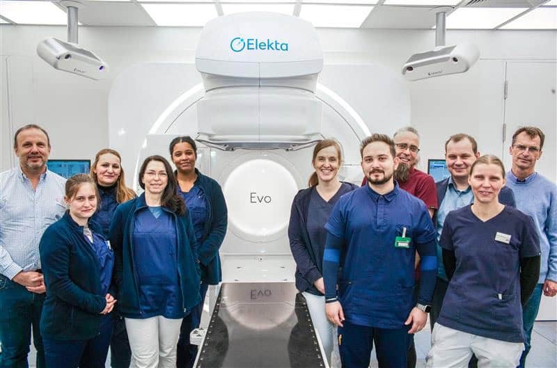
Elekta, the company behind the Unity MR-Linac, believes that in time, all radiation treatments will incorporate ART as standard. Towards this goal, it brings its broad knowledge base from the MR-Linac to the new Elekta Evo, a next-generation CT-Linac designed to improve access to ART. Evo incorporates AI-enhanced cone-beam CT (CBCT), known as Iris, to provide high-definition imaging, while its Elekta ONE Online software automates the entire workflow, including auto-contouring, plan adaptation and end-to-end quality assurance.
A world first
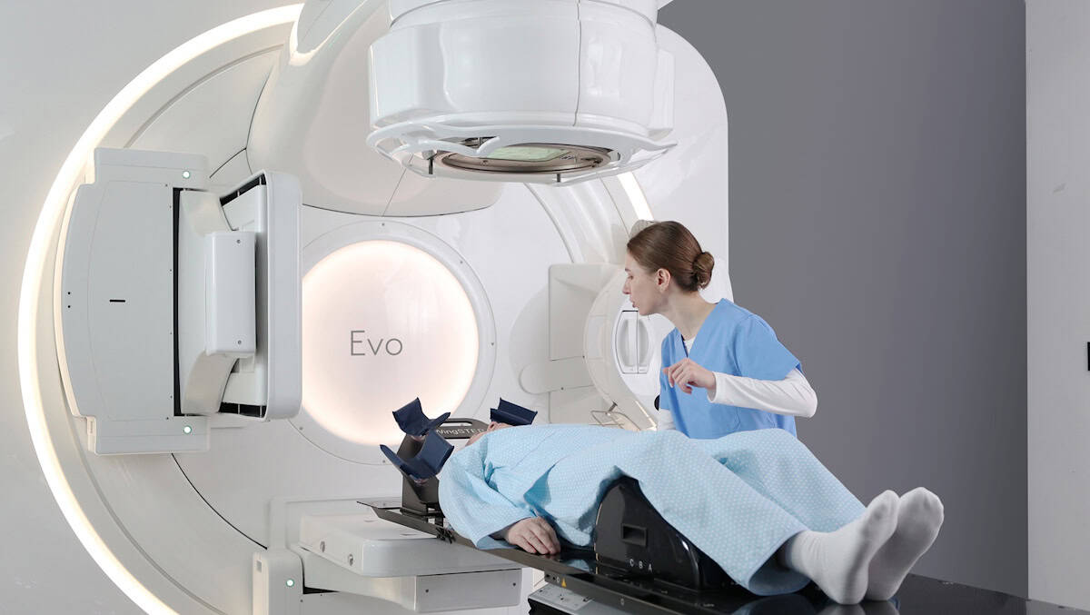
In February of this year, Matthias Lampe and his team at the private centre DTZ Radiotherapy in Berlin, Germany became the first in the world to treat patients with online ART (delivering daily plan updates while the patient is on the treatment couch) using Evo. “To provide proper tumour control you must be sure to hit the target – for that, you need online ART,” Lampe tells Physics World.
Initiating online ART The team at DTZ Radiotherapy in Berlin treated the first patient in the world using Evo. (Courtesy: Elekta)
The ability to visualize and adapt to daily anatomy enables reduction of the planning target volume, increasing safety for nearby organs-at-risk (OARs). “It is highly beneficial for all treatments in the abdomen and pelvis,” says Lampe. “My patients with prostate cancer report hardly any side effects.”
Lampe selected Evo to exploit the full flexibility of its C-arm design. He notes that for the increasingly prevalent hypofractionated treatments, a C-arm configuration is essential. “CT-based treatment planning and AI contouring opened up a new world for radiation oncologists,” he explains. “When Elekta designed Evo, they enabled this in an achievable way with an extremely reliable machine. The C-arm linac is the primary workhorse in radiotherapy, so you have the best of everything.”
Time considerations
While online ART can take longer than conventional treatments, Evo’s use of automation and AI limits the additional time requirement to just five minutes – increasing the overall workflow from 12 to 17 minutes and remaining within the clinic’s standard time slots.
Elekta Evo Evo is a next-generation CT-Linac designed to improve access to adaptive radiotherapy. (Courtesy: Elekta)
The workflow begins with patient positioning and CBCT imaging, with Evo’s AI-enhanced Iris imaging significantly improving image quality, crucial when performing ART. The radiation therapist then matches the cone-beam and planning CTs and performs any necessary couch shift.
Simultaneously, Elekta ONE Online performs AI auto-contouring of OARs, which are reviewed by the physician, and the target volume is copied in. The physicist then simulates the dose distribution on the new contours, followed by a plan review. “Then you can decide whether to adapt or not,” says Lampe. “This is an outstanding feature.” The final stage is treatment delivery and online dosimetry.
When DTZ Berlin first began clinical treatments with Evo, some of Lampe’s colleagues were apprehensive as they were attached to the conventional workflow. “But now, with CBCT providing the chance to see what will be treated, every doctor on my team has embraced the shift and wouldn’t go back,” he says.
The first treatments were for prostate cancer, a common indication that’s relatively easy to treat. “I also thought that if the Elekta ONE workflow struggled, I could contour this on my own in a minute,” says Lampe. “But this was never necessary, the process is very solid. Now we also treat prostate cancer patients with lymph node metastases and those with relapse after radiotherapy. It’s a real success story.”
Lampe says that older and frailer patients may benefit the most from online ART, pointing out that while published studies often include relatively young, healthy patients, “our patients are old, they have chronic heart disease, they’re short of breath”.
For prostate cancer, for example, patients are instructed to arrive with a full bladder and an empty rectum. “But if a patient is in his eighties, he may not be able to do this and the volumes will be different every day,” Lampe explains. “With online adaptive, you can tell patients: ‘if this is not possible, we will handle it, don’t stress yourself’. They are very thankful.”
Making ART available to all
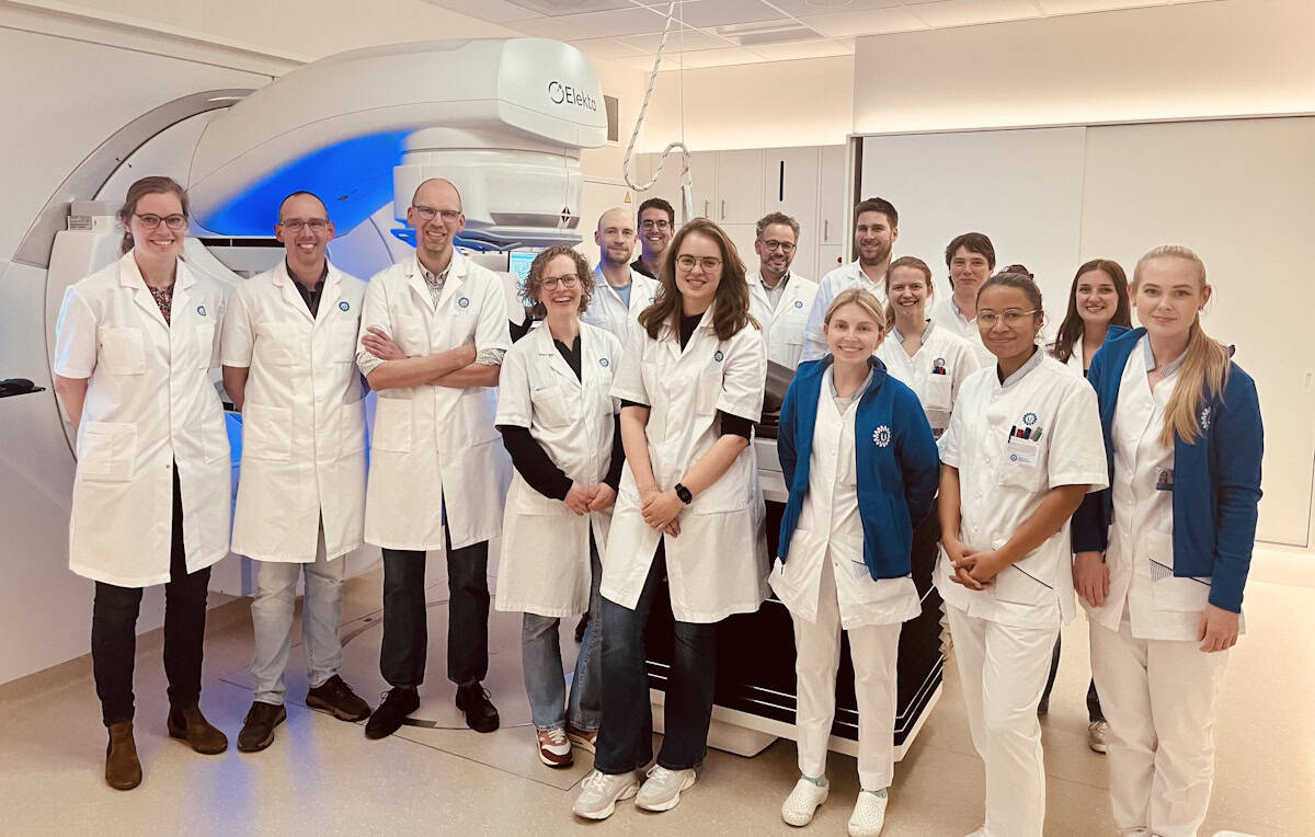
At UMC Utrecht in the Netherlands, the radiotherapy team has also added CT-Linac online adaptive to its clinical toolkit.
UMC Utrecht is renowned for its development of MR-guided radiotherapy, with physicists Bas Raaymakers and Jan Lagendijk pioneering the development of a hybrid MR-Linac. “We come from the world of MR-guidance, so we know that ART makes sense,” says Raaymakers. “But if we only offer MR-guided radiotherapy, we miss out on a lot of patients. We wanted to bring it to the wider community.”
ART for all The radiotherapy team at UMC Utrecht in the Netherlands has added CT-Linac online adaptive to its clinical toolkit. (Courtesy: UMC Utrecht)
At the time of speaking to Physics World, the team was treating its second patient with CBCT-guided ART, and had delivered about 30 fractions. Both patients were treated for bladder cancer, with future indications to explore including prostate, lung and breast cancers and bone metastases.
“We believe in ART for all patients,” says medical physicist Anette Houweling. “If you have MR and CT, you should be able to choose the optimal treatment modality based on image quality. For below the diaphragm, this is probably MR, while for the thorax, CT might be better.”
Ten minute target for OART
Houweling says that ART delivery has taken 19 minutes on average. “We record the CBCT, perform image fusion and then the table is moved, that’s all standard,” she explains. “Then the adaptive part comes in: delineation on the CBCT and creating a new plan with Elekta ONE Planning as part of Elekta One Online.”
The plan adaptation, when selected to perform, takes roughly four minutes to create a clinical-grade volumetric-modulated arc therapy (VMAT) plan. With the soon to be installed next-generation optimizer, it is expected to take less than one minute to generate a VMAT plan.
“As you start with the regular workflow, you can still decide not to choose adaptive treatment, and do a simple couch shift, up until the last second,” says Raaymakers. It’s very close to the existing workflow, which makes adoption easier. Also, the treatment slots are comparable to standard slots. Now with CBCT it takes 19 minutes and we believe we can get towards 10. That’s one of the drivers for cone-beam adaptive.”
Shorter treatment times will impact the decision as to which patients receive ART. If fully automated adaptive treatment is deliverable in a 10-minute time slot, it could be available to all patients. “From the physics side, our goal is to have no technological limitations to delivering ART. Then it’s up to the radiation oncologists to decide which patients might benefit,” Raaymakers explains.
Future gazing
Looking to the future, Raaymakers predicts that simulation-free radiotherapy will be adopted for certain standard treatments. “Why do you need days of preparation if you can condense the whole process to the moment when the patient is on the table,” he says. “That would be very much helped by online ART.”
“Scroll forward a few years and I expect that ART will be automated and fast such that the user will just sign off the autocontours and plan in one, maybe tune a little, and then go ahead,” adds Houweling. “That will be the ultimate goal of ART. Then there’s no reason to perform radiotherapy the traditional way.”
High performance, proven, wire scanner for transverse beam profile measurement for the latest generation of low emittance accelerators and FELs. (Courtesy: UHV Design)
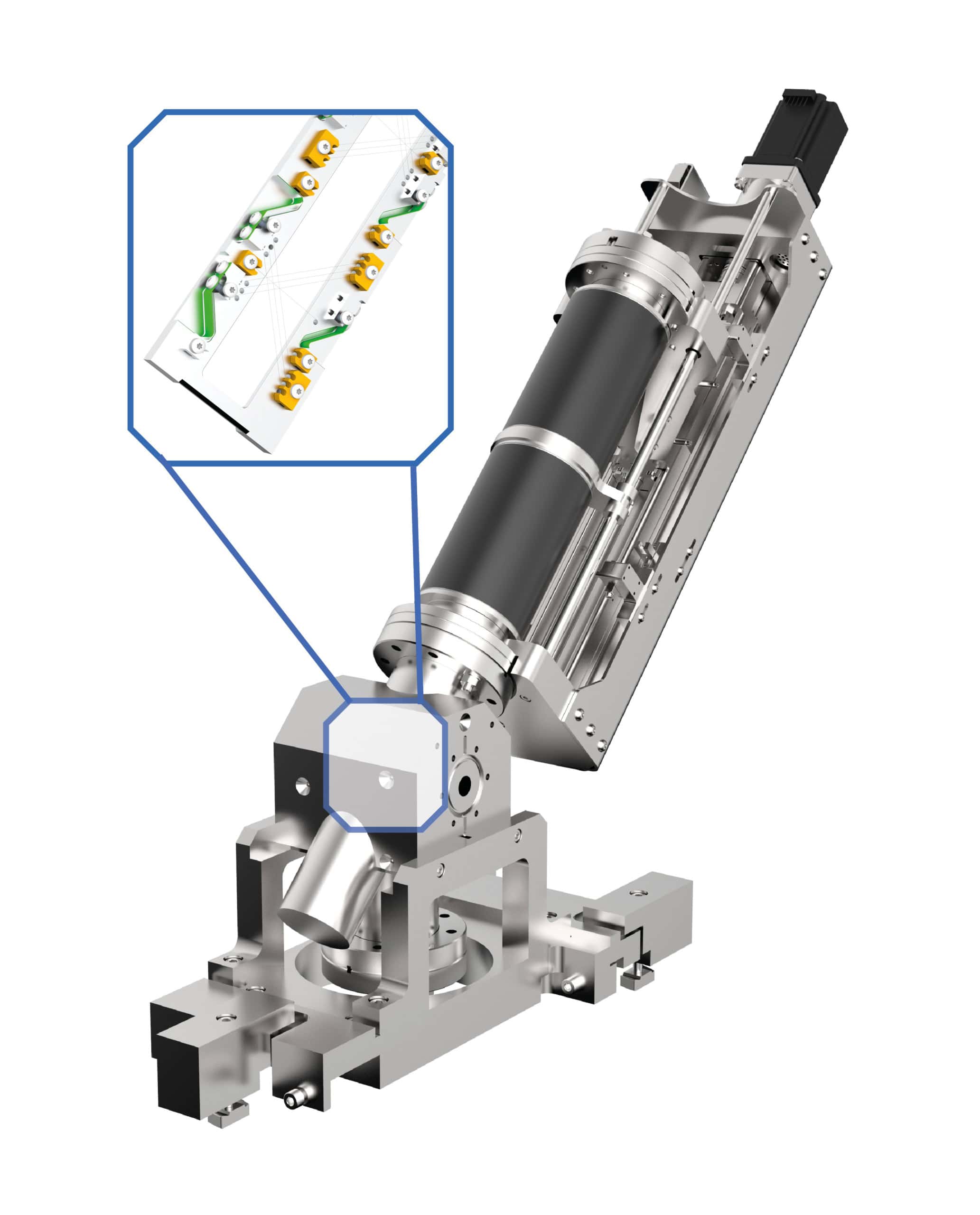
A new high-performance wire scanner fork that the latest generation of free electron lasers (FELs) can use for measuring beam profiles has been developed by UK-based firm UHV Design. Produced using technology licensed from the Paul Scherrer Institute (PSI) in Switzerland, the device could be customized for different FELs and low emittance accelerators around the world. It builds on the company’s PLSM range, which allows heavy objects to be moved very smoothly and with minimal vibrations.
The project began 10 years ago when the PSI was starting to build the Swiss Free Electron Laser and equipping the facility, explains Jonty Eyres. The remit for UHV Design was to provide a stiff, very smooth, bellows sealed, ultra-high vacuum compatible linear actuator that could move a wire fork without vibrating it adversely. The fork, designed by PSI, can hold wires in two directions and can therefore scan the intensity of the beam profile in both X and Y planes using just one device as opposed to two or more as in previous such structures.
“We decided to employ an industrial integrated ball screw and linear slide assembly with a very stiff frame around it, the construction of which provides the support and super smooth motion,” he says. “This type of structure is generally not used in the ultra-high vacuum industry.”
The position of the wire fork is determined through a (radiation-hard) side mounted linear optical encoder in conjunction with the PSI’s own motor and gearbox assembly. A power off brake is also incorporated to avoid any issues with back driving under vacuum load if electrical power was to be lost to the PLSM. All electrical connections terminated with UTO style connectors to PSI specification.
Long term reliability was important to avoid costly and unnecessary down time, particularly between planned FEL maintenance shutdowns. The industrial ball screw and slide assembly by design was the perfect choice in conjunction with a bellows assembly rated for 500,000 cycles with an option to increase to 1 million cycles.
Eyres and his UHV design team began by building a prototype that the PSI tested themselves with a high-speed camera. Once validated, the UHV engineers then built a batch of 20 identical units to prove that the device could be replicated in terms of constraints and tolerances.
The real challenge in constructing this device, says Eyres, was about trying to minimize the amount of vibration on the wire, which, for PSI, is typically between 5 and 25 microns thick. This is only possible if the vibration of the wire during a scan is low compared to the cross section of the wire – that is, about a micron for a 25-micron wire. “Otherwise, you are just measuring noise,” explains Eyres. “The small vibration we achieved can be corrected for in calculations, so providing an accurate value for the beam profile intensity.”
UHV Design holds the intellectual property rights for the linear actuator and PSI the property rights of the fork. Following the success of the project and a subsequent agreement between them both, it was recently decided that UHV Design buy the licence to promote the wire fork, allowing the company to sell the device or a version of it to any institution or company operating a FEL or low-emittance accelerator. “The device is customizable and can be adapted to different types of fork, wires, motors or encoders,” says Eyres. “The heart of the design remains the same: a very stiff structure and its integrated ball screw and linear slide assembly. But, it can be tailored to meet the requirements of different beam lines in terms of stroke size, specific wiring and the components employed.”
UHV Design’s linear actuator was installed on the Swiss FEL in 2016 and has been performing very well since, says Eyres.
A final and important point to note, he adds, is that UHV Design built an identical copy of their actuator when we took on board the licence agreement, so that we could prove it could still reproduce the same performance. “We built an exact copy of the wire scanner, including the PSI fork assembly and sent it to the PSI, who then used the very same high-speed camera rig that they’d employed in 2015 to directly compare the new actuator with the original ones supplied. They reported that the results were indeed comparable, meaning that if fitted to the Swiss FEL today, it would perform in the same way.”
Silicon-based lithium-ion batteries exhibit severe time-based degradation resulting in poor calendar lives. In this webinar, we will talk about how calendar aging is measured, why the traditional measurement approaches are time intensive and there is a need for new approaches to optimize materials for next generation silicon based systems. Using this new approach we also screen multiple new electrolyte systems that can lead to calendar life improvements in Si containing batteries.
An interactive Q&A session follows the presentation.
Ankit Verma
Ankit Verma’s expertise is in physics-based and data-driven modeling of lithium-ion and next generation lithium metal batteries. His interests lie in unraveling the coupled reaction-transport-mechanics behavior in these electrochemical systems with experiment-driven validation to provide predictive insights for practical advancements. Predominantly, he’s working on improving silicon anodes energy density and calendar life as part of the Silicon Consortium Project, understanding solid-state battery limitations and upcycling of end-of-life electrodes as part of the ReCell Center.
Verma’s past works include optimization of lithium-ion battery anodes and cathodes for high-power and fast-charge applications and understanding electrodeposition stability in metal anodes.
Brain metastases – cancerous lesions that have spread from elsewhere in the body – are increasingly treated using stereotactic radiotherapy (SRS), a precision technique that targets each individual lesion with a high dose of radiation. Compared with whole-brain irradiation, SRS may lead to higher local control and increased cognitive sparing, as well as a shorter overall treatment duration. But to target and treat multiple brain metastases, each lesion must first be detected on an MRI scan and accurately delineated. And this can be a complex and time-consuming task.
“There are two challenges that we face in the clinic,” explains Evrim Tezcanli, professor of radiation oncology at Acibadem Atasehir Hospital in Turkey. “First, we want to treat all the lesions. But very small lesions, particularly those under 0.1 cc, can easily be missed by untrained eyes. Larger metastases, meanwhile, are more challenging to contour – you want to cover the whole lesion without missing a pixel, but don’t want to spill radiation over into the brain tissue. It’s time-consuming work, especially if there are multiple lesions.”
To address these challenges, Siemens Healthineers has developed an AI-powered software tool that automates the contouring of brain metastases. The software – integrated into the company’s syngo.via RT Image Suite and AI-Rad Companion Organs RT packages – employs advanced deep-learning algorithms to rapidly analyse a patient’s MR images and contour and label metastatic lesions. Alongside, it delineates key organs at risk, such as the brainstem and optic structures.
“One of the main strengths of this software is that it reduces the manual workloads really well,” says Tezcanli.
Meeting clinical standards
To evaluate the accuracy and time efficiency of the new software tool, Tezcanli and her team compared AI-based delineation with the performance of two experienced radiation oncologists. The study included data from 10 patients with between three and 17 brain metastases. The radiation oncologists manually contoured all lesions (82 in total) based on patients’ contrast-enhanced MRI scans; the same images were also processed by the AI software to automatically contour the metastases.
Tezcanli reports that the software performed remarkably well. “One of the most significant findings was that the manual contours and the AI-generated contours showed strong agreement, especially for lesions larger than 0.1 cc. In terms of geometric similarity, the AI-generated boundaries were well within our clinically acceptable levels,” she says.
Comparing the manual and AI-generated contours revealed a medium Dice similarity coefficient of 0.83, increasing to 0.91 when excluding very small lesions, and a median Hausdorff distance (the maximum distance between the two contours) of 0.3 mm.
AI will definitely have a place because of the time savings and accuracy it delivers
Evrim Tezcanli
To quantify the overall time efficiency, the researchers timed the contouring process for the radiation oncologists and the AI tool. They also measured the time taken for expert review of the AI-generated results, in which a radiation oncologist checks the contours and performs any necessary adjustments before they are approved for treatment planning.
The AI software completed the contouring for each patient in just one to two minutes, reducing the workload by an average of 75%, and in some cases saving over 30 minutes per patient. “We still needed to review the AI contours, but the correction time was only three to four minutes,” says Tezcanli, emphasizing that expert review remains essential when using AI. “One case required nine minutes, but even with that patient we had a time saving of 75%.”
As well as saving time for the oncology staff, AI-based contouring has a lot to offer from the patient’s perspective. Spending less time on demanding manual contouring frees up the physician to spend more time with the patient.
Lesion detection
For their study, the researchers analysed post-contrast T1 MPRAGE sequences recorded using a 3 Tesla MRI scanner. To maximize lesion enhancement, they acquired images several minutes after contrast injection, though Tezcanli notes that this timing may vary between treatment centres. They also used image slices of 1 mm or less. “This is a very precise treatment and we want to make sure everything is accurate,” she adds.
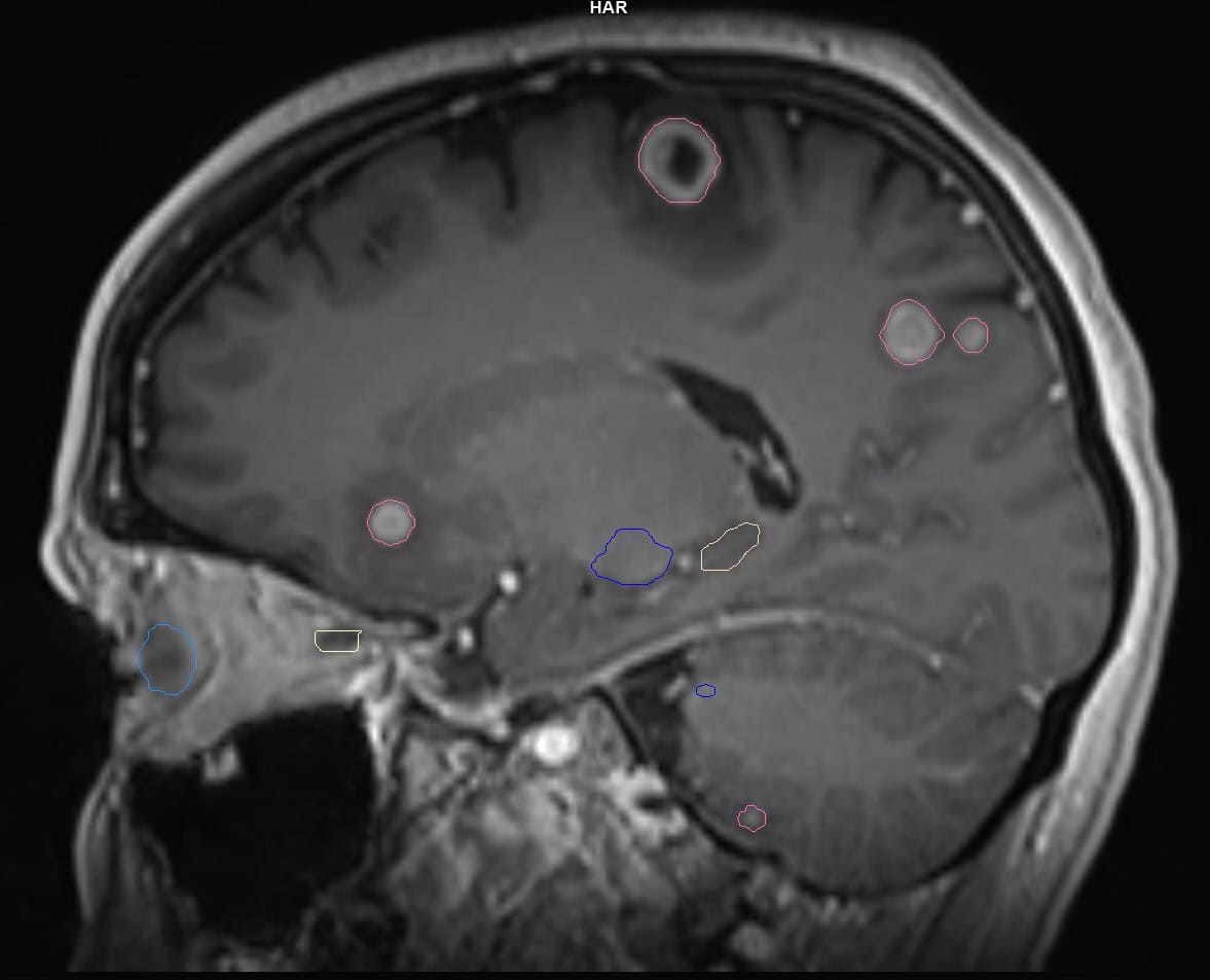
Reducing manual workload Autocontouring of brain metastases on an MR image. (Courtesy: Acibadem Atasehir Hospital, Istanbul, Turkey)
The study deliberately included patients with varying numbers of different sized metastases, to assess the algorithms under diverse clinical scenarios. In terms of lesion detection, the software exhibited an overall sensitivity of 94% – finding 77 of the 82 metastases. The five missed lesions were extremely small, 0.01 to 0.03 cc, a volume that’s challenging even for physicians to detect. The software did, however, find three additional lesions that were not originally identified and which were later confirmed as brain metastases.
The false positive rate was 8.5%, with the software mistakenly identifying seven vascular structures as metastases. “Because the algorithms work with contrast enhancement, any vascular enhancements that mimic the tumour can be mistaken,” says Tezcanli. “Here we needed to use a dedicated MRI sequence to define whether it was a metastasis or not. That’s just one thing to be cautious about. Other than that, we were very satisfied with the software’s ability to detect small lesions and find ones that we hadn’t detected.”
Automation with HyperArc
The contours generated by the AI software are exported in DICOM RT Struct format, enabling direct transfer into the treatment planning system. At Acibadem Atasehir Hospital, this next step is performed using HyperArc, a radiosurgery-specific software module within the Eclipse treatment planning infrastructure. HyperArc performs automated treatment planning and delivery, enabling fast and efficient SRS on the Varian TrueBeam and Edge linacs.
“HyperArc has proven to be highly effective, even when treating patients with multiple brain metastases,” says Burcin Ispir, a medical physicist working alongside Tezcanli. “One of its biggest powers is its ability to perform single isocentre, automated planning for multiple targets, which significantly reduces planning time while maintaining excellent plan quality. In our experience, HyperArc-generated plans offer high conformity and steep dose gradients, which are critical for sparing normal brain tissue.”
Unlike conventional radiotherapy where homogeneity is desirable, SRS plans intentionally allow controlled heterogeneity within the target volume to improve sparing of normal tissue. HyperArc also offers automation of the beam geometry, including collimator and couch angles, ensuring consistent, fast and highly reproducible plans “For selected cases, we have found this enables a same-day workflow where contouring, planning and treatment can all be completed within a single day,” Ispir explains.
The automation in AI contouring and HyperArc planning speeds up the treatment planning process, and when compared to traditional workflows, potentially allows patients to commence radiation therapy treatments earlier. The ability to commence treatment as soon as possible after the MRI scan is imperative when treating brain metastases. Most patients will also be receiving systemic therapies, which need to be delivered on schedule. But perhaps more importantly, the high spatial precision of SRS makes the technique sensitive to even small anatomical changes within lesions. If the delay between MR imaging and radiotherapy treatment is too long, any changes occurring during that time could decrease targeting accuracy.
“We are in an era where we are using the technology to have even same-day treatments,” says Tezcanli. “We have rapid contouring with AI, a quick review of a few minutes by the expert radiation oncologist, treatment planning with HyperArc, and then a few hours later the patient is treated. This is where the technology is taking us.”
Look to the future
Continuing improvements in cancer treatment techniques mean that patients are living longer, but this also increases the likelihood of metastases developing. In addition, higher quality MRI scans and enhanced imaging protocols lead to more metastases being detected. These factors combine to increase the workload on centres treating multiple metastases with SRS.
“I think we will be treating brain metastasis more and more,” says Tezcanli. “And I think radiosurgery will be the main treatment modality in the future. AI will definitely have a place because of the time savings and accuracy it delivers. And this is only the first version of the software; I’m sure it can be improved to find even smaller lesions or differentiate vascular structures.”
Following the initial software evaluation, the team has not yet fully integrated it into their clinical routine, but Tezcanli tells Physics World that they would be happy to use the software in every one of their brain metastases treatments. “I think we will be using it routinely in the future in all of our clinical cases,” she says.
The statements by customers of Siemens Healthineers described herein are based on results that were achieved in the customer’s unique setting. Because there is no “typical” hospital or laboratory and many variables exist (e.g., hospital size, samples mix, case mix, level of IT and/or automation adoption) there can be no guarantee that other customers will achieve the same results.
The products/features mentioned herein are not commercially available in all countries. Their future availability cannot be guaranteed.
Autocontouring results are generated by Siemens. The displayed renderings are created with software that is not commercially available.
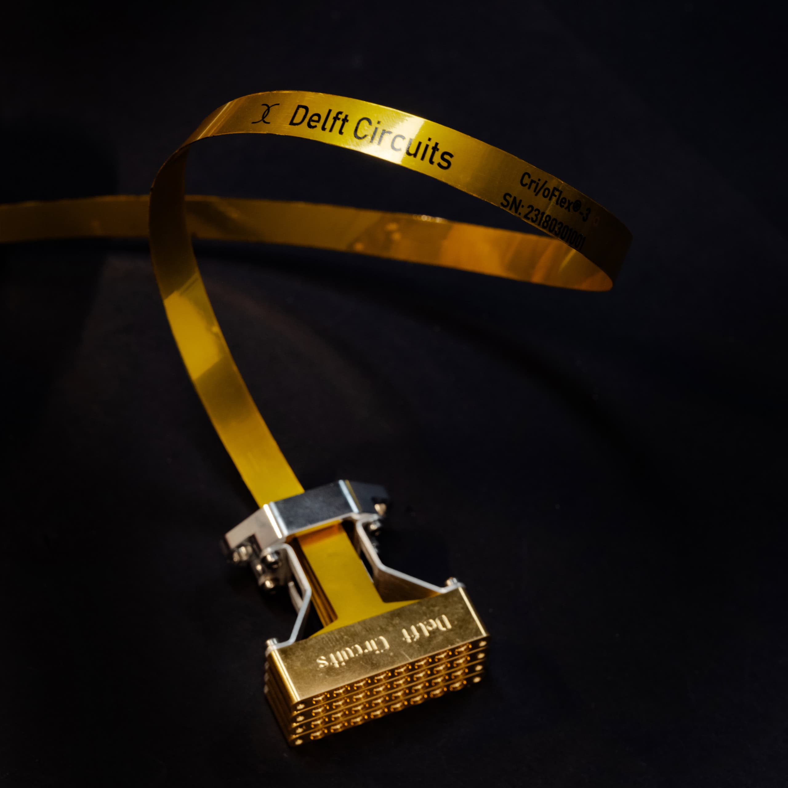
Flexible thinking, scalable innovation Delft Circuits has established itself as a one-stop shop for scalable cryogenic I/O assemblies in quantum computing. The company’s Cri/oFlex® cabling platform combines fully integrated filtering with a compact footprint and low heatload. (Courtesy: Delft Circuits)
As manufacturers in the nascent quantum supply chain turn their gaze towards at-scale commercial opportunities in quantum computing, the scenic city of Delft in the Netherlands is emerging as a heavyweight player in quantum science, technology and innovation. At the heart of this regional quantum ecosystem is Delft Circuits, a Dutch manufacturer of specialist I/O cabling solutions, which is aligning its product development roadmap to deliver a core enabling technology for the scale-up and industrial deployment of next-generation quantum computing, communications and sensing systems.
Kuitenbrouwer “Cri/oFlex® allows us to increase the I/O cabling density easily – and by a lot.” (Courtesy: Delft Circuits)
In brief, the company’s Cri/oFlex® cryogenic RF cables comprise a stripline (a type of transmission line) based on planar microwave circuitry – essentially a conducting strip encapsulated in dielectric material and sandwiched between two conducting ground planes. The use of the polyimide Kapton® as the dielectric ensures Cri/oFlex® cables remain flexible in cryogenic environments (which are necessary to generate quantum states, manipulate them and read them out), with silver or superconducting NbTi providing the conductive strip and ground layer. The standard product comes as a multichannel flex (eight channels per flex) with a range of I/O channel configurations tailored to the customer’s application needs, including flux bias lines, microwave drive lines, signal lines or read-out lines.
“As quantum computers evolve – think more and more qubits plus increasingly exacting requirements on gate fidelity – system developers will reach a point where current coax cabling technology doesn’t cut it anymore,” explains Daan Kuitenbrouwer, co-founder of Delft Circuits. “The key to our story is that Cri/oFlex® allows us to increase the I/O cabling density easily – and by a lot – to scale the number of channels in a single system while guaranteeing high gate fidelities [minimizing noise and heating] as well as market-leading uptime and reliability.”
Quantum alignment
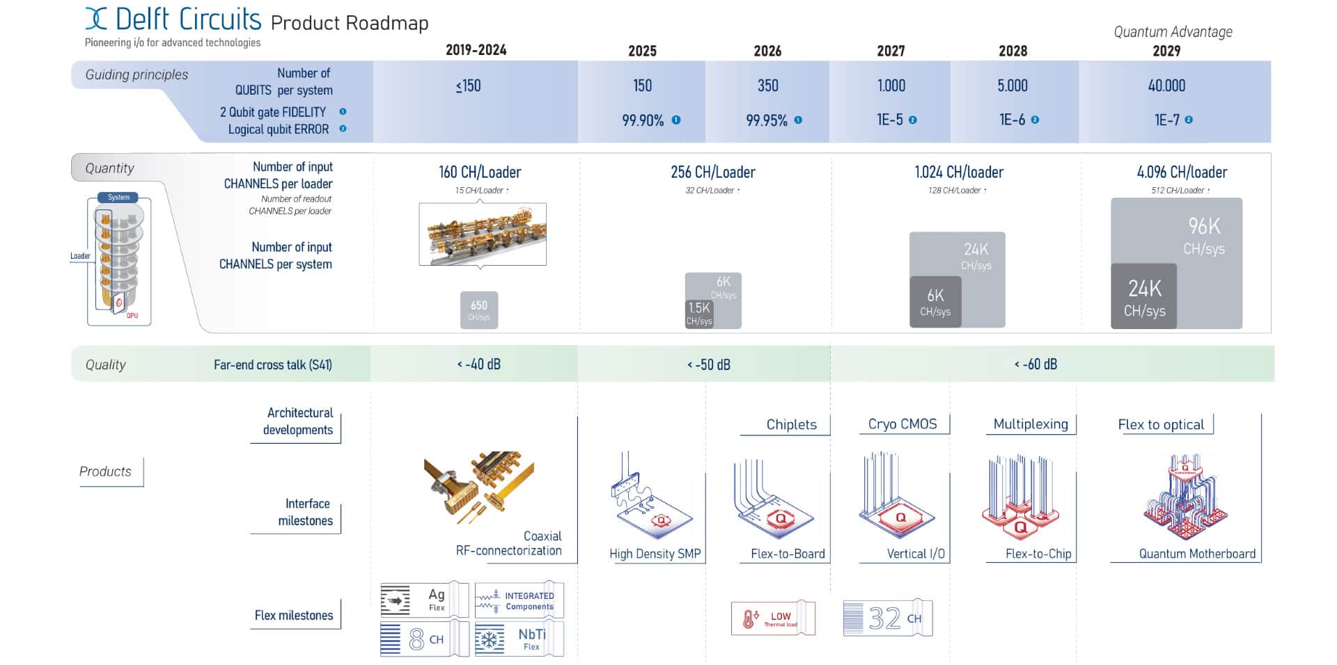
To put some hard-and-fast performance milestones against that claim, Kuitenbrouwer and colleagues have just published a granular product development roadmap that aligns Cri/oFlex® cabling specifications against the anticipated evolution of quantum computing systems – from 150+ qubits today out to 40,000 qubits and beyond in 2029 (see figure, “Quantum alignment”).
Quantum alignment The new product development roadmap from Delft Circuits starts with the guiding principles, highlighting performance milestones to be achieved by the quantum computing industry over the next five years – specifically, the number of physical qubits per system and gate fidelities. By extension, cabling metrics in the Delft Circuits roadmap focus on “quantity”: the number of I/O channels per loader (i.e. the wiring trees that insert into a cryostat, with typical cryostats having between 6–24 slots for loaders) and the number of channels per cryostat (summing across all loaders); also on “quality” (the crosstalk in the cabling flex). To complete the picture, the roadmap outlines product introductions at a conceptual level to enable both the quantity and quality timelines. (Courtesy: Delft Circuits)
“Our roadmap is all about enabling, from an I/O perspective, the transition of quantum technologies out of the R&D lab into at-scale practical applications,” says Kuitenbrouwer. “As such, we studied the development roadmaps of more than 10 full-stack quantum computing vendors to ensure that our ‘guiding principles’ align versus the aggregate view of quantity and quality of qubits targeted by the system developers over time.”
Notwithstanding the emphasis on technology innovation and continuous product improvement, Delft Circuits is also “coming of age” in line with the wider quantum community. Most notably, the company’s centre of gravity is shifting inexorably from academic end-users to servicing vendors large and small in the quantum supply chain. “What we see are full-stack quantum computing companies starting to embrace horizontal thinking – which, in our case, means a technology partner able to solve their entire I/O cabling challenge,” explains Kuitenbrouwer.
To gain traction, however, systems integrators at the sub-stack level must, as a given, design their product offering with industrial metrics front-and-centre – for example, scalability, manufacturability, reliability, cost per I/O channel and second-sourcing. Equally important is the need to forge long-term vendor-customer relationships that often move beyond the transactional into the realm of co-development and collaboration – though all against a standardized package of cabling options.
“We integrate Cri/oFlex® with cryostats that have relatively standard vacuum feedthroughs and thermalization – more or less the same across the board,” says Kuitenbrouwer. What changes is the type of qubit – superconducting, spin, photonic – which in turn determines the configuration of the I/O line and where to place the attenuators, low-pass filters and IR filters. “This is something we can adjust relatively easily – at high volume and high reliability – with the whole I/O package installed and tested at the customer premises,” he adds.
Timing is key for quantum advantage
Commercially, Delft Circuits is already making real headway, getting “in the door” with many of the leading developers of quantum computing systems in North America and Europe. One of the main reasons for that is the ability to respond to customer requirements in an agile and timely fashion, argues Sal Bosman, a fellow co-founder of Delft Circuits.
Bosman “Currently, we are the only industrial supplier able to deliver flexible circuits of superconducting materials at scale.” (Courtesy: Delft Circuits)
“We work on the basis of a very structured design process, playing to our strengths in superconductor fabrication, integrated microwave components and cryogenic engineering,” Bosman notes. “We have also developed our own in-house software to simulate the performance of Cri/oFlex® cabling in full-stack quantum systems. No other vendor can match this level of customer support and attention to detail.”
Right now, though, it’s all about momentum as Delft Circuits seeks to capitalize on its first-mover advantage and, what Bosman claims, is the unique value proposition of its Cri/oFlex® technology: a complete and inherently scalable I/O solution with integrated flex cables incorporating filters and high-density interconnects to quantum chips or control electronics.
With this in mind, the company is busy constructing a new 750m2 clean-room (with an option to double that footprint) alongside its existing 1000m2 in-house pilot-production and test facility. “Currently, we are the only industrial supplier able to deliver flexible circuits of superconducting materials at scale,” concludes Bosman.
“Over the next two to three years,” he adds, “we have a credible opportunity to grab significant market share when it comes to cabling I/O for quantum. Watch this space: a lot of customers are already coming to us saying ‘we don’t want to buy more coax, we want to work with you.’”
Location, location, location
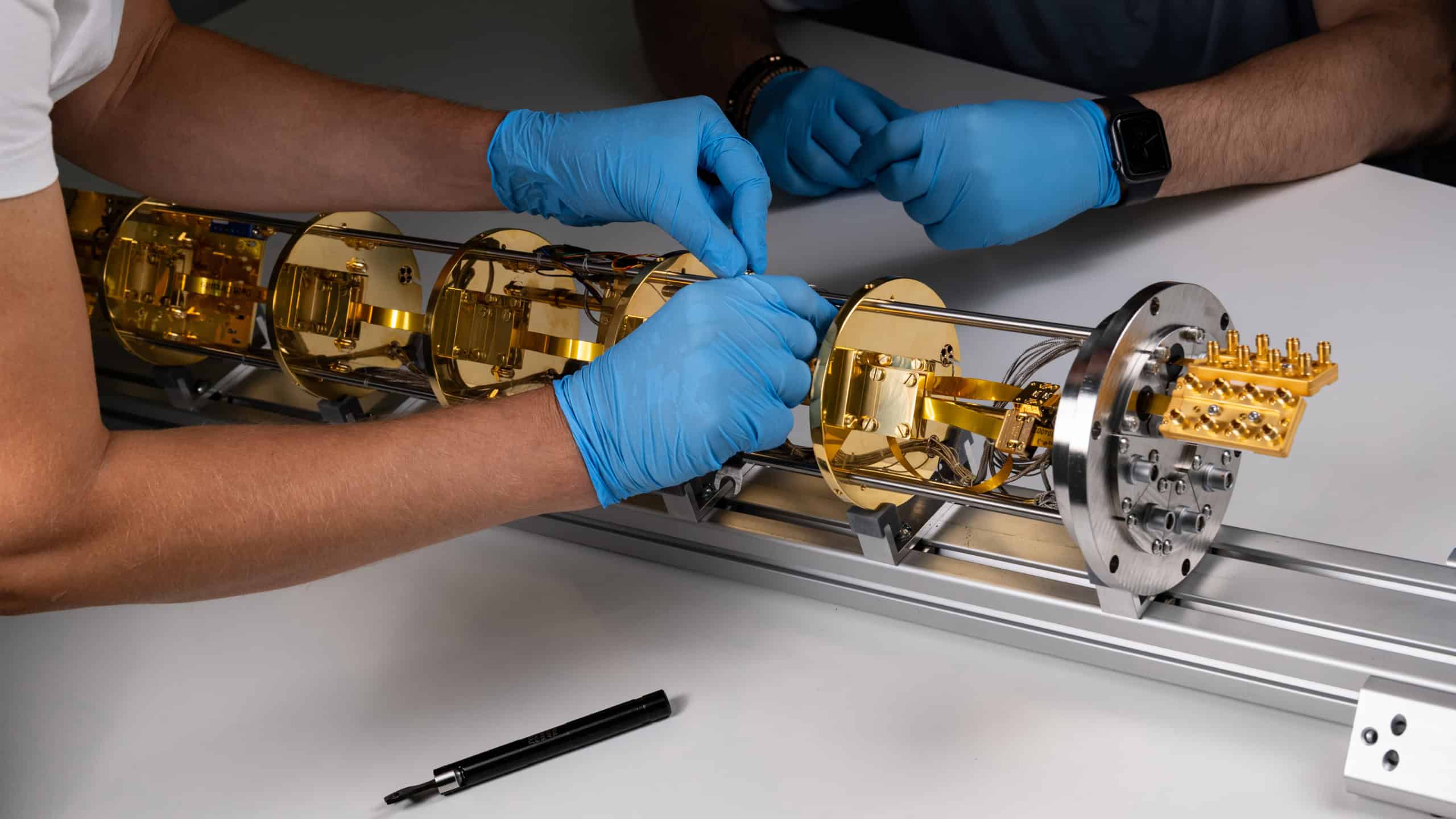
Cryogenic integration Delft Circuits can supply fully pre-assembled loaders with Cri/oFlex® cabling inside. (Courtesy: Delft Circuits)
Delft Circuits sits within a thriving regional cluster for quantum science and technology called Quantum Delta Delft, which is centred around the canal-ringed city of Delft between The Hague and Rotterdam.
Formed in 2017 and initially located at the Faculty of Applied Sciences at Delft University of Technology (TU Delft), Delft Circuits has since grown as an independent company and is now based in the historic Cable District, where its facilities include a dedicated fabrication, pilot-production and testing area.
TU Delft is itself home to a high-profile interfaculty research institute called QuTech, a collaboration with the Netherlands Organisation for Applied Scientific Research (TNO) that’s tasked with developing full-stack hardware and software layers (including enhanced qubit technologies) for quantum computing and quantum communications systems.
Alongside this academic powerhouse, the Delft region has seen the emergence of other quantum tech start-ups like QuantWare (quantum chips), Qblox (control electronics) and Orange Quantum Systems (test solutions). All three companies work closely with Delft Circuits as part of the ImpaQT UA cooperative, a joint effort to develop open standards and interoperable technologies that enable system integrators to build quantum computing hardware stacks from off-the-shelf components.
“The ImpaQT UA story is ongoing,” explains Kuitenbrouwer. “As partners, we are super-complementary and collaborate closely to shape the future of quantum computing.” That’s why the new development roadmap is so important for Delft Circuits: to communicate a vision from the “component layer” up the value chain to the full-stack quantum computing companies.
As well as the talent pipeline that comes with proximity to TU Delft and QuTech, Quantum Delta Delft is home to TNO’s Quantum Information Technology Testing (QITT) Facility, which enables European companies to evaluate their cryogenic or non-cryogenic quantum devices and software in a full-stack quantum computing set-up.
Radiotherapy is a precision cancer therapy that employs personalized treatment plans to target radiation to tumours with high accuracy. Such plans are usually created from high-resolution CT scans of the patient. But interest is growing in an alternative approach: MR simulation, in which MR images are used to generate the treatment plans – for delivery on conventional linac systems as well as the increasingly prevalent MR-guided radiotherapy systems.
One site that has transitioned to this approach is the Institut Jules Bordet in Belgium, which in 2021 acquired both an Elekta Unity MR-Linac and a Siemens MAGNETOM Aera MR-Simulator. “It was a long-term objective for our clinic to have an MR-only workflow,” says Akos Gulyban, a medical physicist at Institut Jules Bordet. “When we moved to a new campus, we decided to purchase the MR-Linac. Then we thought that if we are getting into the MR world for treatment adaptation, we also need to step up in terms of simulation.”
The move to MR simulation delivers many clinical benefits, with MR images providing the detailed anatomical information required to delineate targets and organs-at-risk with the highest precision. But it also creates new challenges for the physicists, particularly when it comes to quality assurance (QA) of MR-based systems. “The biggest concern is geometric distortion,” Gulyban explains. “If there is no distortion correction, then the usability of the machine or the sequence is very limited.”
Addressing distortion
While the magnetic field gradient is theoretically linear, and MRI is indeed extremely accurate at the imaging isocentre, moving away from the isocentre increases distortion. Images of regions 30 or 40 cm away from the isocentre – a reasonable distance for a classical linac – can differ from reality by 15 to 20 mm, says Gulyban. Thankfully, 3D correction algorithms can reduce this discrepancy down to just a couple of millimetres. But such corrections first require an accurate way to measure the distortion.
Akos Gulyban: “The biggest concern is geometric distortion.” (Courtesy: Bordet – Service Communication)
To address this task, the team at Institut Jules Bordet employ a geometric distortion phantom –the QUASAR MRID3D Geometric Distortion Analysis System from IBA Dosimetry. Gulyban explains that the MRID3D was chosen following discussions with experienced users, and that key selling points included the phantom’s automated software and its ability to efficiently store results for long-term traceability.
“My concern was how much time we spend cross-processing, generating reports or evaluating results,” he says. “This software is fully automated, making it much easier to perform the evaluation and less dependent on the operator.”
Gulyban adds that the team was looking for a vendor-independent solution. “I think it is a good approach to use the tools provided [by the vendor] but now we have a way to measure the same thing using a different approach. Since our new campus has a mixture of Siemens MRs and the MR-Linac, this phantom provides a vendor-independent bridge between the two worlds.”
For quality control of the MR-Simulator, the team perform distortion measurements every three months, as well as after system interventions such as shimming and following any problems arising during other routine QA procedures. “We should not consider tests as individual islands in the QA process,” says Gulyban. “For instance, the ACR image quality phantom, which is used for more frequent evaluation, also partly assesses distortion. If we see that failing, I would directly trigger measurements with the more appropriate geometric distortion phantom.”
A lightweight option
To perform MR simulation, the images used for treatment planning must encompass both the target volume and the surrounding region, to ensure accurate delineation of the tumour and nearby organs-at-risk. This requires a large field-of-view (FOV) scan – plus geometric distortion QA that covers the same large FOV.
Kawtar Lakrad: “The idea behind the phantom was very smart.” (Courtesy: Kawtar Lakrad)
“You’re using this image to delineate the target and also to spare the organs-at-risk, so the image must reflect reality,” explains Kawtar Lakrad, medical physicist and clinical application specialist at IBA Dosimetry. “You don’t want that image to be twisted or the target volume to appear smaller or bigger than it actually is. You want to make sure that all geometric qualities of the image align with what’s real.”
Typically, geometric distortion phantoms are grid-like, with control points spaced every 0.5 or 1 cm. The entire volume is imaged in the MR scanner and the locations of control points seen in the image compared with their actual positions. “If we apply this to a large FOV phantom, which for MRI will be filled with either water or oil, it’s going to be a very large grid and it’s going to be heavy, 40 or 50 kg,” says Lakrad.
To overcome this obstacle, IBA researchers used innovative harmonic analysis algorithms to design a lightweight geometric distortion phantom with submillimetre accuracy and a large (35 x 30 cm) FOV: the MRID3D. The phantom comprises two concentric hollow acrylic cylinders, the only liquid being a prefilled mineral oil layer between the two shells, reducing its weight to just 21 kg.
Lightweight and accurate The MRID3D geometric distortion phantom in use on the treatment couch. (Courtesy: IBA Dosimetry)
“The idea behind the phantom was very smart because it relies on a mathematical tool,” explains Lakrad. “There is a Fourier transform for the linear signal, which is used for standard grids. But there are also spherical harmonics – and this is what’s used in the MRID3D. The control points are all on the cylinder surface, plus one in the isocentre, creating a virtual grid that measures 3D geometric distortion.” She adds that the MRID3D can also differentiate distortion due to the main magnetic field from gradient non-linearity distortion.
Moving into the MR world
Gulyban and his team at Institut Jules Bordet first used MR simulation for pelvic treatments, particularly prostate cancer, he tells Physics World. This was followed by abdominal tumours, such as pancreatic and liver cancers (where many patients were being treated on the MR-Linac) and more recently, cranial and head-and-neck irradiations.
Gulyban points out that the introduction of the MR-Simulator was eased by the team’s experience with the MR-Linac, which helped them “step into the MR world”. Here also, the MRID3D phantom is used to quantify geometric distortion, both for initial commissioning and continuous QA of the MR-Linac.
Screen shot B0 distortion mapping with MRID3D. (Courtesy: IBA Dosimetry)
“It’s like a consistency check,” he explains. “We have certain manufacturer-defined conditions that we need to meet for the MR-Linac – for instance, that distortion within a 40 mm diameter should be less than 1 mm. To ensure that these are met in a consistent fashion, we repeat the measurements with the manufacturer’s phantom and with the MRID3D. This gives us extra peace of mind that the machine is performing under the correct conditions.”
For other cancer centres looking to integrate MR into their radiotherapy clinics, Gulyban has some key points of advice. These include starting with MR-guided radiotherapy and then adding MR simulation, identifying a suitable pathology to treat first and gain familiarity, and attending relevant courses or congresses for inspiration.
“The biggest change is actually a change in culture because you have an active MRI in the radiotherapy department,” he notes. “We are used to the radioprotection aspects of radiotherapy, wearing a dosimeter and observing radiation protection principles. MRI is even less forgiving – every possible thing that could go wrong you have to eliminate. Closing all the doors and emptying your pockets must become a reflex habit. You have to prepare mentally for that.”
“When you’re used to CT-based machines, moving to an MR workflow can be a little bit new,” adds Lakrad. “Most physicists are already familiar with the MR concept, but when it comes to the QA process, that’s the most challenging part. Some people would just repeat what’s done in radiology – but the use case is different. In radiotherapy, you have to delineate the target and surrounding volumes exactly. You’re going to be delivering dose, which means the tolerance between diagnostic and radiation therapy is different. That’s the biggest challenge.”