AMD RX 9070 XT Review ft. ASRock
Officially announced – at long last! – in a livestreamed event last week, AMD's RDNA 4 architecture is here with the RX 9070 XT leading the charge. Landing with a $599 MSRP, this GPU is firmly targeting Nvidia's RTX 5070 Ti, with AMD promising compelling rasterisation performance alongside huge improvements to ray tracing. FSR 4 also touts significant image quality improvements thanks to its new ML-powered algorithm, so on paper AMD looks to have ticked all the boxes. But how does that translate into the real world experience? We find out today…
Timestamps:
00:00 Intro
00:41 Recap and spec overview
01:48 Test setup
03:02 Alan Wake 2
03:41 Black Myth: Wukong
04:11 Cyberpunk 2077
04:14 Final Fantasy XVI
05:14 Forza Horizon 5
05:47 Ghost of Tsushima
06:21 Horizon Forbidden West
06:54 The Last of Us Part 1
07:20 Plague Tale: Requiem
07:42 Senua’s Saga: Hellblade 2
08:09 Starfield
08:36 Total War: Warhammer III
08:55 12-game average results
10:57 Cost per frame analysis
11:55 RT Alan Wake II
12:28 RT Black Myth: Wukong
12:57 RT Cyberpunk 2077
13:19 RT F1 24
13:40 RT Ratchet & Clank
14:00 RT Returnal
14:12 RT Shadow of the Tomb Raider
14:23 RT Star Wars Outlaws
14:43 RT 8-game average
15:18 FSR 4 analysis
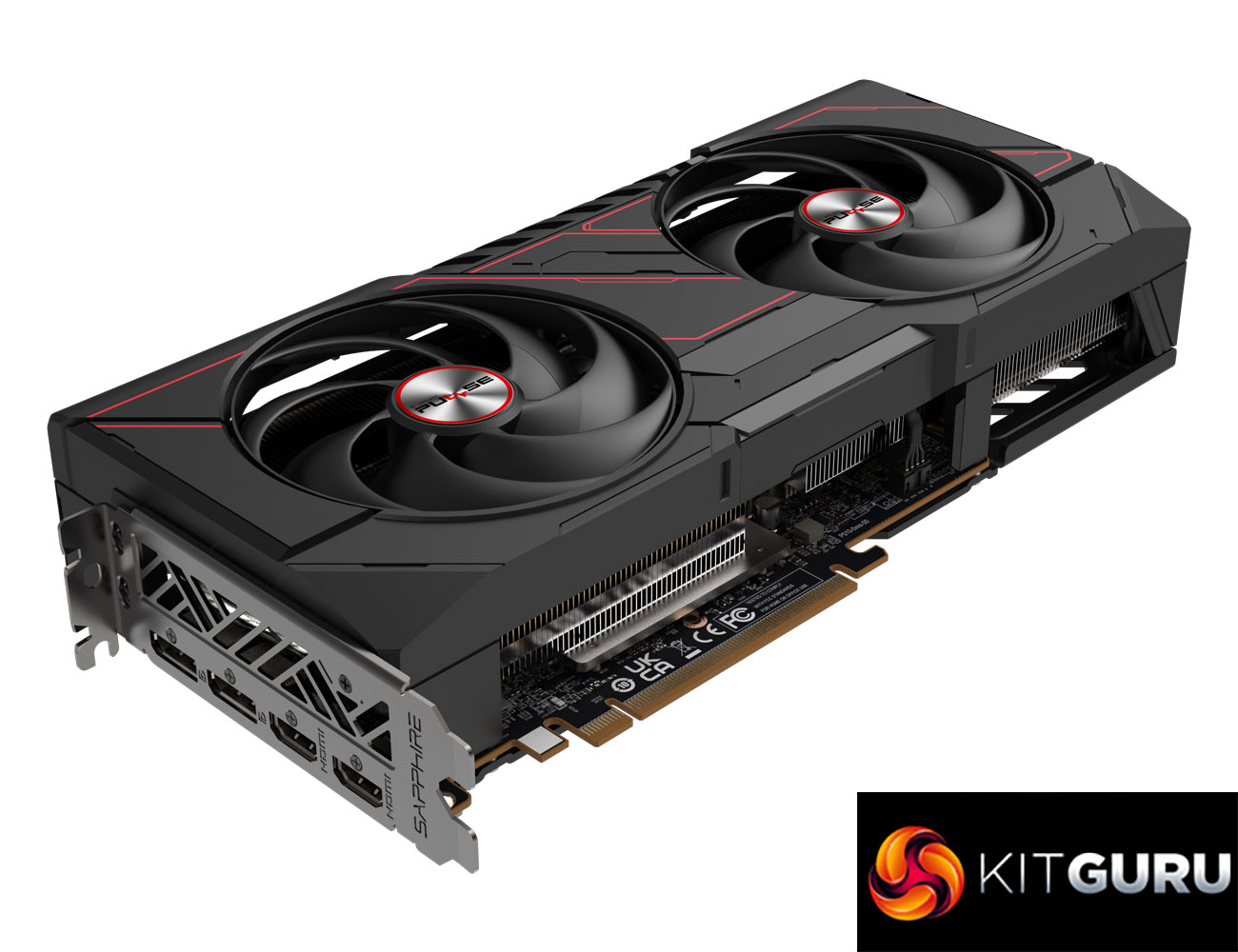
18:56 Meet the Sapphire Pulse & ASRock Taichi
20:19 Thermals and acoustics
21:24 Power draw and efficiency
23:18 Closing thoughts
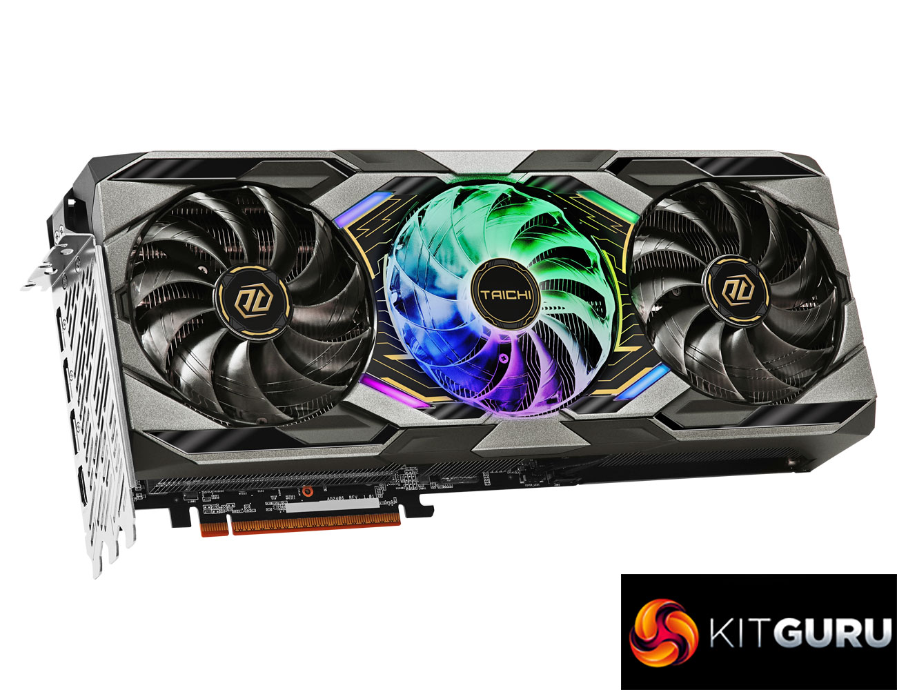
In lieu of an official AMD reference (or MBA) card, today we are using the ASRock RX 9070 XT Taichi for our testing. This card does come factory overclocked when using the default Gaming BIOS, but I did all my testing with the Quiet BIOS that runs at reference specifications.
It's also worth noting that while this is a standalone review for the RX 9070 XT, we do have a day one review for the RX 9070 (non-XT), and you can find that HERE.
| RX 9070 XT | RX 9070 | RX 7900 GRE | RX 7800 XT | RX 7700 XT | |
| Architecture | RDNA 4 | RDNA 4 | RDNA 3 | RDNA 3 | RDNA 3 |
| Manufacturing Process | TSMC N4 | TSMC N4 | TSMC N5 GCD + N6 MCD | TSMC N5 GCD + N6 MCD | TSMC N5 GCD + N6 MCD |
| Transistor Count | 53.9 billion | 53.9 billion | 57.7 billion | 28.1 billion | 28.1 billion |
| Die Size | 357 mm² | 357 mm² | 300 mm² GCD
220 mm² MCD |
200 mm² GCD
150 mm² MCD |
200 mm² GCD
150 mm² MCD |
| Compute Units | 64 | 56 | 80 | 60 | 54 |
| Ray Accelerators | 64 | 56 | 80 | 60 | 54 |
| Stream Processors | 4096 | 3584 | 5120 | 3840 | 3456 |
| Game GPU Clock | 2400 MHz | 2070 MHz | 1880 MHz | 2124 MHz | 2171 MHz |
| Boost GPU Clock | Up to 2970 MHz | Up to 2520 MHz | Up to 2245 MHz | Up to 2430 MHz | Up to 2544 MHz |
| ROPs | 128 | 128 | 192 | 96 | 96 |
| AMD Infinity Cache | 64MB | 64MB | 64MB | 64MB | 48MB |
| Memory | 16GB GDDR6 | 16GB GDDR6 | 16GB GDDR6 | 16GB GDDR6 | 12GB GDDR6 |
| Memory Data Rate | 20 Gbps | 20 Gbps | 18 Gbps | 19.5 Gbps | 18 Gbps |
| Memory Bandwidth | 645 GB/s | 645 GB/s | 576 GB/s | 624 GB/s | 432 GB/s |
| Memory Interface | 256-bit | 256-bit | 256-bit | 256-bit | 192-bit |
| Board Power | 304W | 220W | 260 W | 263W | 245W |

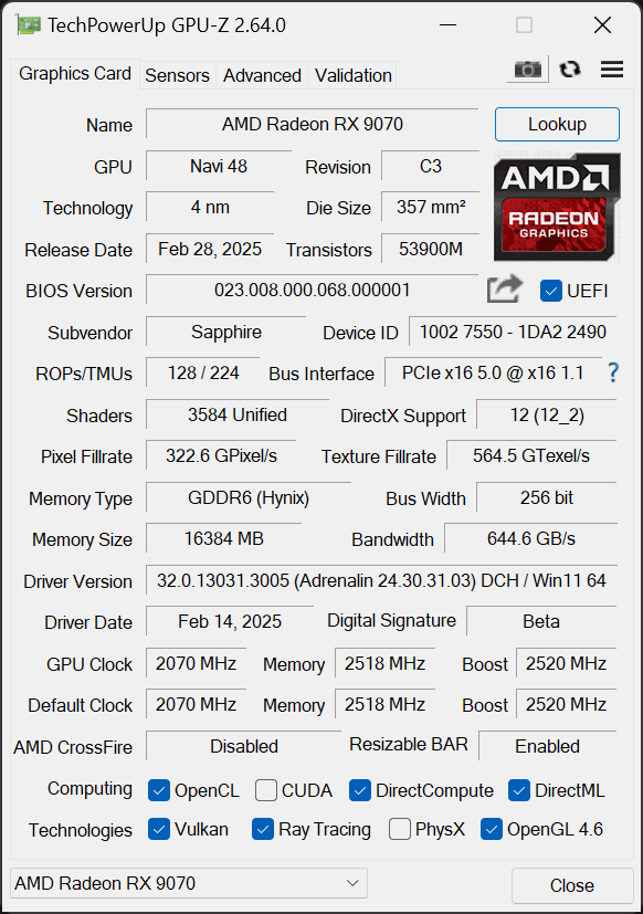
First, let's take a quick look at the specs. The RX 9070 XT is built on the new Navi 48 die, measuring 357mm², and it's worth pointing out this is a monolithic chip, so AMD is not using a chiplet-based design as per RDNA 3. In total, Navi 48 silicon packs in 53.9 billion transistors.
As a full implementation of Navi 48, the RX 9070 XT packs in 64 Compute Units, and each CU houses 64 Steam Processors, for a total of 4096 shaders. There's also 64 Ray Accelerators – one per CU – and 128 ROPs.
As for clock speed, the RX 9070 XT runs notably faster than its sibling, the RX 9070, given it sports a rated game clock of 2400MHz and a boost clock of up to 2970MHz.
The memory configuration is the same between both GPUs though, with 16GB of GDDR6 memory clocked at 20Gbps, operating over a 256-bit memory interface, for total memory bandwidth of 645 GB/s. 64MB of Infinity Cache is also present.
Power draw for the RX 9070 XT rated at 304W Total Board Power (TBP), but we are using our updated GPU power testing methodology in this review, so read on for our most detailed power and efficiency testing yet.
The post AMD RX 9070 XT Review ft. ASRock first appeared on KitGuru.