Physicists at the University of Stuttgart, Germany have teleported a quantum state between photons generated by two different semiconductor quantum dot light sources located several metres apart. Though the distance involved in this proof-of-principle “quantum repeater” experiment is small, members of the team describe the feat as a prerequisite for future long-distance quantum communications networks.
“Our result is particularly exciting because such a quantum Internet will encompass these types of distant quantum nodes and will require quantum states that are transmitted among these different nodes,” explains Tim Strobel, a PhD student at Stuttgart’s Institute of Semiconductor Optics and Functional Interfaces (IHFG) and the lead author of a paper describing the research. “It is therefore an important step in showing that remote sources can be effectively interfaced in this way in quantum teleportation experiments.”
In the Stuttgart study, one of the quantum dots generates a single photon while the other produces a pair of photons that are entangled – meaning that the quantum state of one photon is closely linked to the state of the other, no matter how far apart they are. One of the photons in the entangled pair then travels to the other quantum dot and interferes with the photon there. This process produces a superposition that allows the information encapsulated in the single photon to be transferred to the distant “partner” photon from the pair.
Quantum frequency converters
Strobel says the most challenging part of the experiment was making photons from two remote quantum dots interfere with each other. Such interference is only possible if the two particles are indistinguishable, meaning they must be similar in every regard, be it in their temporal shape, spatial shape or wavelength. In contrast, each quantum dot is unique, especially in terms of its spectral properties, and each one emits photons at slightly different wavelengths.
To close the gap, the team used devices called quantum frequency converters to precisely tune the wavelength of the photons and match them spectrally. The researchers also used the converters to shift the original wavelengths of the photons emitted from the quantum dots (around 780 nm) to a wavelength commonly used in telecommunications (1515 nm) without altering the quantum state of the photons. This offers further advantages: “Being at telecommunication wavelengths makes the technology compatible with the existing global optical fibre network, an important step towards real-life applications,” Strobel tells Physics World.
Proof-of-principle experiment
In this work, the quantum dots were separated by an optical fibre just 10 m in length. However, the researchers aim to push this to considerably greater distances in the future. Strobel notes that the Stuttgart study was published in Nature Communications back-to-back with an independent work carried out by researchers led by Rinaldo Trotta of Sapienza University in Rome, Italy. The Rome-based group demonstrated quantum state teleportation across the Sapienza University campus at shorter wavelengths, enabled by the brightness of their quantum-dot source.
“These two papers that we published independently strengthen the measurement outcomes, demonstrating the maturity of quantum dot light sources in this domain,” Strobel says. Semiconducting quantum dots are particularly attractive for this application, he adds, because as well as producing both single and entangled photons on demand, they are also compatible with other semiconductor technologies.
Fundamental research pays off
Simone Luca Portalupi, who leads the quantum optics group at IHFG, notes that “several years of fundamental research and semiconductor technology are converging into these quantum teleportation experiments”. For Peter Michler, who led the study team, the next step is to leverage these advances to bring quantum-dot-based teleportation technology out of a controlled laboratory environment and into the real world.
Strobel points out that there is already some precedent for this, as one of the group’s previous studies showed that they could maintain photon entanglement across a 36-km fibre link deployed across the city of Stuttgart. “The natural next step would be to show that we can teleport the state of a photon across this deployed fibre link,” he says. “Our results will stimulate us to improve each building block of the experiment, from the sample to the setup.”
The 2026 SPIE Photonics West meeting takes place in San Francisco, California, from 17 to 22 January. The premier event for photonics research and technology, Photonics West incorporates more than 100 technical conferences covering topics including lasers, biomedical optics, optoelectronics, quantum technologies and more.
As well as the conferences, Photonics West also offers 60 technical courses and a new Career Hub with a co-located job fair. There are also five world-class exhibitions featuring over 1500 companies and incorporating industry-focused presentations, product launches and live demonstrations. The first of these is the BiOS Expo, which begins on 17 January and examines the latest breakthroughs in biomedical optics and biophotonics technologies.
Then starting on 20 January, the main Photonics West Exhibition will host more than 1200 companies and showcase the latest innovative optics and photonics devices, components, systems and services. Alongside, the Quantum West Expo features the best in quantum-enabling technology advances, the AR | VR | MR Expo brings together leading companies in XR hardware and systems and – new for 2026 – the Vision Tech Expo highlights cutting-edge vision, sensing and imaging technologies.
Here are some of the product innovations on show at this year’s event.
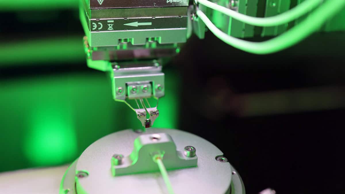
Enabling high-performance photonics assembly with SmarAct
As photonics applications increasingly require systems with high complexity and integration density, manufacturers face a common challenge: how to assemble, align and test optical components with nanometre precision – quickly, reliably and at scale. At Photonics West, SmarAct presents a comprehensive technology portfolio addressing exactly these demands, spanning optical assembly, fast photonics alignment, precision motion and advanced metrology.
Rapid and reliable SmarAct’s technology portfolio enables assembly, alignment and testing of optical components with nanometre precision. (Courtesy: SmarAct)
A central highlight is SmarAct’s Optical Assembly Solution, presented together with a preview of a powerful new software platform planned for release in late-Q1 2026. This software tool is designed to provide exceptional flexibility for implementing automation routines and process workflows into user-specific control applications, laying the foundation for scalable and future-proof photonics solutions.
For high-throughput applications, SmarAct showcases its Fast Photonics Alignment capabilities. By combining high-dynamic motion systems with real-time feedback and controller-based algorithms, SmarAct enables rapid scanning and active alignment of PICs and optical components such as fibres, fibre array units, lenses, beam splitters and more. These solutions significantly reduce alignment time while maintaining sub-micrometre accuracy, making them ideal for demanding photonics packaging and assembly tasks.
Both the Optical Assembly Solution and Fast Photonics Alignment are powered by SmarAct’s electromagnetic (EM) positioning axes, which form the dynamic backbone of these systems. The direct-drive EM axes combine high speed, high force and exceptional long-term durability, enabling fast scanning, smooth motion and stable positioning even under demanding duty cycles. Their vibration-free operation and robustness make them ideally suited for high-throughput optical assembly and alignment tasks in both laboratory and industrial environments.
Precision feedback is provided by SmarAct’s advanced METIRIO optical encoder family, designed to deliver high-resolution position feedback for demanding photonics and semiconductor applications. The METIRIO stands out by offering sub-nanometre position feedback in an exceptionally compact and easy-to-integrate form factor. Compatible with linear, rotary and goniometric motion systems – and available in vacuum-compatible designs – the METIRIO is ideally suited for space-constrained photonics setups, semiconductor manufacturing, nanopositioning and scientific instrumentation.
For applications requiring ultimate measurement performance, SmarAct presents the PICOSCALE Interferometer and Vibrometer. These systems provide picometre-level displacement and vibration measurements directly at the point of interest, enabling precise motion tracking, dynamic alignment, and detailed characterization of optical and optoelectronic components. When combined with SmarAct’s precision stages, they form a powerful closed-loop solution for high-yield photonics testing and inspection.
Together, SmarAct’s motion, metrology and automation solutions form a unified platform for next-generation photonics assembly and alignment.
Visit SmarAct at booth #3438 at Photonics West and booth #8438 at BiOS to discover how these technologies can accelerate your photonics workflows.
Avantes previews AvaSoftX software platform and new broadband light source
Photonics West 2026 will see Avantes present the first live demonstration of its completely redesigned software platform, AvaSoftX, together with a sneak peek of its new broadband light source, the AvaLight-DH-BAL. The company will also run a series of application-focused live demonstrations, highlighting recent developments in laser-induced breakdown spectroscopy (LIBS), thin-film characterization and biomedical spectroscopy.
AvaSoftX is developed to streamline the path from raw spectra to usable results. The new software platform offers preloaded applications tailored to specific measurement techniques and types, such as irradiance, LIBS, chemometry and Raman. Each application presents the controls and visualizations needed for that workflow, reducing time and the risk of user error.
Streamlined solution The new AvaSoftX software platform offers next-generation control and data handling. (Courtesy: Avantes)
Smart wizards guide users step-by-step through the setup of a measurement – from instrument configuration and referencing to data acquisition and evaluation. For more advanced users, AvaSoftX supports customization with scripting and user-defined libraries, enabling the creation of reusable methods and application-specific data handling. The platform also includes integrated instruction videos and online manuals to support the users directly on the platform.
The software features an accessible dark interface optimized for extended use in laboratory and production environments. Improved LIBS functionality will be highlighted through a live demonstration that combines AvaSoftX with the latest Avantes spectrometers and light sources.
Also making its public debut is the AvaLight-DH-BAL, a new and improved deuterium–halogen broadband light source designed to replace the current DH product line. The system delivers continuous broadband output from 215 to 2500 nm and combines a more powerful halogen lamp with a reworked deuterium section for improved optical performance and stability.
A switchable deuterium and halogen optical path is combined with deuterium peak suppression to improve dynamic range and spectral balance. The source is built into a newly developed, more robust housing to improve mechanical and thermal stability. Updated electronics support adjustable halogen output, a built-in filter holder, and both front-panel and remote-controlled shutter operation.
The AvaLight-DH-BAL is intended for applications requiring stable, high-output broadband illumination, including UV–VIS–NIR absorbance spectroscopy, materials research and thin-film analysis. The official launch date for the light source, as well as the software, will be shared in the near future.
Avantes will also run a series of live application demonstrations. These include a LIBS setup for rapid elemental analysis, a thin-film measurement system for optical coating characterization, and a biomedical spectroscopy demonstration focusing on real-time measurement and analysis. Each demo will be operated using the latest Avantes hardware and controlled through AvaSoftX, allowing visitors to assess overall system performance and workflow integration. Avantes’ engineering team will be available throughout the event.
For product previews, live demonstrations and more, meet Avantes at booth #1157.
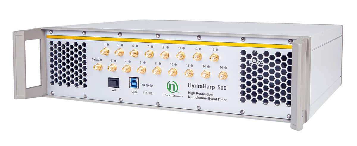
HydraHarp 500: high-performance time tagger redefines precision and scalability
One year after its successful market introduction, the HydraHarp 500 continues to be a standout highlight at PicoQuant’s booth at Photonics West. Designed to meet the growing demands of advanced photonics and quantum optics, the HydraHarp 500 sets benchmarks in timing performance, scalability and flexible interfacing.
At its core, the HydraHarp 500 delivers exceptional timing precision combined with ultrashort jitter and dead time, enabling reliable photon timing measurements even at very high count rates. With support for up to 16 fully independent input channels plus a common sync channel, the system allows true simultaneous multichannel data acquisition without cross-channel dead time, making it ideal for complex correlation experiments and high-throughput applications.
At the forefront of photon timing The high-resolution multichannel time tagger HydraHarp 500 offers picosecond timing precision. It combines versatile trigger methods with multiple interfaces, making it ideally suited for demanding applications that require many input channels and high data throughput. (Courtesy: PicoQuant)
A key strength of the HydraHarp 500 is its high flexibility in detector integration. Multiple trigger methods support a wide range of detector technologies, from single-photon avalanche diodes (SPADs) to superconducting nanowire single-photon detectors (SNSPDs). Versatile interfaces, including USB 3.0 and a dedicated FPGA interface, ensure seamless data transfer and easy integration into existing experimental setups. For distributed and synchronized systems, White Rabbit compatibility enables precise cross-device timing coordination.
Engineered for speed and efficiency, the HydraHarp 500 combines ultrashort per-channel dead time with industry-leading timing performance, ensuring complete datasets and excellent statistical accuracy even under demanding experimental conditions.
Looking ahead, PicoQuant is preparing to expand the HydraHarp family with the upcoming HydraHarp 500 L. This new variant will set new standards for data throughput and scalability. With outstanding timing resolution, excellent timing precision and up to 64 flexible channels, the HydraHarp 500 L is engineered for highest-throughput applications powered – for the first time – by USB 3.2 Gen 2×2, making it ideal for rapid, large-volume data acquisition.
With the HydraHarp 500 and the forthcoming HydraHarp 500 L, PicoQuant continues to redefine what is possible in photon timing, delivering precision, scalability and flexibility for today’s and tomorrow’s photonics research. For more information, visit www.picoquant.com or contact us at info@picoquant.com.
Meet PicoQuant at BiOS booth #8511 and Photonics West booth #3511.
Physicists in the UK have succeeded in routing and teleporting entangled states of light between two four-user quantum networks – an important milestone in the development of scalable quantum communications. Led by Mehul Malik and Natalia Herrera Valencia of Heriot-Watt University in Edinburgh, Scotland, the team achieved this milestone thanks to a new method that uses light-scattering processes in an ordinary optical fibre to program a circuit. This approach, which is radically different from conventional methods based on photonic chips, allows the circuit to function as a programmable entanglement router that can implement several different network configurations on demand.
The team performed the experiments using commercially-available optical fibres, which are multi-mode structures that scatter light via random linear optical processes. In simple terms, Herrera Valencia explains that this means the light tends to ricochet chaotically through the fibres along hundreds of internal pathways. While this effect can scramble entanglement, researchers at the Institut Langevin in Paris, France had previously found that the scrambling can be calculated by analysing how the fibre transmits light. What is more, the light-scattering processes in such a medium can be harnessed to make programmable optical circuits – which is exactly what Malik, Herrera Valencia and colleagues did.
“Top-down” approach
The researchers explain that this “top-down” approach simplifies the circuit’s architecture because it separates the layer where the light is controlled from the layer in which it is mixed. Using waveguides for transporting and manipulating the quantum states of light also reduces optical losses. The result is a reconfigurable multi-port device that can distribute quantum entanglement between many users simultaneously in multiple patterns, switching between different channels (local connections, global connections or both) as required.
A further benefit is that the channels can be multiplexed, allowing many quantum processors to access the system at the same time. The researchers say this is similar to multiplexing in classical telecommunications networks, which makes it possible to send huge amounts of data through a single optical fibre using different wavelengths of light.
Access to a large number of modes
Although controlling and distributing entangled states of light is key for quantum networks, Malik says it comes with several challenges. One of these is that conventional methods based on photonics chips cannot be scaled up easily. They are also very sensitive to imperfections in how they’re made. In contrast, the waveguide-based approach developed by the Heriot-Watt team “opens up access to a large number of modes, providing significant improvements in terms of achievable circuit size, quality and loss,” Malik tells Physics World, adding that the approach also fits naturally with existing optical fibre infrastructures.
Gaining control over the complex scattering process inside a waveguide was not easy, though. “The main challenge was the learning curve and understanding how to control quantum states of light inside such a complex medium,” Herrera Valencia recalls. “It took time and iteration, but we now have the precise and reconfigurable control required for reliable entanglement distribution, and even more so for entanglement swapping, which is essential for scalable networks.”
While the Heriot-Watt team used the technique to demonstrate flexible quantum networking, Malik and Herrera Valencia say it might also be used for implementing large-scale photonic circuits. Such circuits could have many applications, ranging from machine learning to quantum computing and networking, they add.
Looking ahead, the researchers, who report their work in Nature Photonics, say they are now aiming to explore larger-scale circuits that can operate on more photons and light modes. “We would also like to take some of our network technology out of the laboratory and into the real world,” says Malik, adding that Herrera Valencia is leading a commercialization effort in that direction.
An effect first observed decades ago by Nobel laureate Arthur Ashkin has been used to fine tune the electrical charge on objects held in optical tweezers. Developed by an international team led by Scott Waitukaitis of the Institute of Science and Technology Austria, the new technique could improve our understanding of aerosols and clouds.
Optical tweezers use focused laser beams to trap and manipulate small objects about 100 nm to 1 micron in size. Their precision and versatility have made them a staple across fields from quantum optics to biochemistry.
Ashkin shared the 2018 Nobel prize for inventing optical tweezers and in the 1970s he noticed that trapped objects can be electrically charged by the laser light. “However, his paper didn’t get much attention, and the observation has essentially gone ignored,” explains Waitukaitis.
Waitukaitis’ team rediscovered the effect while using optical tweezers to study how charges build up in the ice crystals accumulating inside clouds. In their experiment, micron-sized silica spheres stood in for the ice, but Ashkin’s charging effect got in their way.
Bummed out
“Our goal has always been to study charged particles in air in the context of atmospheric physics – in lightning initiation or aerosols, for example,” Waitukaitis recalls. “We never intended for the laser to charge the particle, and at first we were a bit bummed out that it did so.”
Their next thought was that they had discovered a new and potentially useful phenomenon. “Out of due diligence we of course did a deep dive into the literature to be sure that no one had seen it, and that’s when we found the old paper from Ashkin, “ says Waitukaitis.
In 1976, Ashkin described how optically trapped objects become charged through a nonlinear process whereby electrons absorb two photons simultaneously. These electrons can acquire enough energy to escape the object, leaving it with a positive charge.
Yet beyond this insight, Ashkin “wasn’t able to make much sense of the effect,” Waitukaitis explains. “I have the feeling he found it an interesting curiosity and then moved on.”
Shaking and scattering
To study the effect in more detail, the team modified their optical tweezers setup so its two copper lens holders doubled as electrodes, allowing them to apply an electric field along the axis of the confining, opposite-facing laser beams. If the silica sphere became charged, this field would cause it to shake, scattering a portion of the laser light back towards each lens.
The researchers picked off this portion of the scattered light using a beam splitter, then diverted it to a photodiode, allowing them to track the sphere’s position. Finally, they converted the measured amplitude of the shaking particle into a real-time charge measurement. This allowed them to track the relationship between the sphere’s charge and the laser’s tuneable intensity.
Their measurements confirmed Ashkin’s 1976 hypothesis that electrons on optically-trapped objects undergo two-photon absorption, allowing them to escape. Waitukaitis and colleagues improved on this model and showed how the charge on a trapped object can be controlled precisely by simply adjusting the laser’s intensity.
As for the team’s original research goal, the effect has actually been very useful for studying the behaviour of charged aerosols.
“We can get [an object] so charged that it shoots off little ‘microdischarges’ from its surface due to breakdown of the air around it, involving just a few or tens of electron charges at a time,” Waitukaitis says. “This is going to be really cool for studying electrostatic phenomena in the context of particles in the atmosphere.“
Team effort Based at the University of Innsbruck, Ben Lanyon’s group has created a novel qubit register by trapping ten ions. (Courtesy: Victor Krutyanskiy/University of Innsbruck)
Researchers in Austria have entangled matter-based qubits with photonic qubits in a ten-ion system. The technique is scalable to larger ion-qubit registers, paving the way for the creation of larger and more complex quantum networks.
Ions in motion Each ion (large object) is moved one at a time into the “sweet spot” of the optical cavity. Once there, a laser beam drives the emission of a single photon (small object), entangled with the ion. The colours indicate ion–photon entanglement. (Courtesy: Universität Innsbruck/Harald Ritsch)
Quantum networks consist of matter-based nodes that store and process quantum information and are linked through photons (quanta of light). Already, Ben Lanyon’s group at the University of Innsbruck has made advances in this direction by entangling two ions in different systems. Now, in a new paper published in Physical Review Letters , they describe how they have developed and demonstrated a new method to entangle a string of ten ions with photons. In the future, this approach could enable the entanglement of sets of ions in different locations through light, rather than one ion at a time.
To achieve this, Lanyon and colleagues trapped a chain of 10 calcium ions in a linear trap in an optical cavity. By changing the trapping voltages in the trap, each ion was moved, one-by-one, into the cavity. Once inside, the ion was placed in the “sweet spot”, where the ion’s interaction with the cavity is the strongest. There, the ion emitted a single photon when exposed to a 393 nm Raman laser beam. This beam was tightly focused on one ion, guaranteeing that the emitted photon – collected in a single-mode optical fibre – comes out from one ion at a time. This process was carried out ten times, one per ion, to obtain a train of ten photons.
By using quantum state tomography, the researchers reconstructed the density matrix, which describes the correlation between the states of ions (i) and photons (j). To do so, they measure every ion and photon state in three different basis, resulting in nine Pauli-basis configurations of quantum measurements. From the density matrix, the concurrence (a measure of entanglement) between the ion (i) and photon (j) was found to be positive only when i = j, and equal to zero otherwise. This implies that the ion is uniquely entangled with the photon it produced, and unentangled with the photon produced by other ions.
From the density matrix, they also calculate the fidelity with the Bell state (a state of maximum entanglement), yielding an average 92%. As Marco Canteri points out, “this fidelity characterizes the quality of entanglement between the ion-photon pair for i=j”.
This work developed and demonstrated a technique whereby matter-based qubits and photonic qubits can be entangled, one at a time, in ion strings. Now, the group aims to “demonstrate universal quantum logic within the photon-interfaced 10-ion register and, building up towards entangling two remote 10-ion processors through the exchange of photons between them,” explains team member Victor Krutyanskiy. If this method effectively scales to larger systems, more complex quantum networks could be built. This would lead to applications in quantum communication and quantum sensing.