China launched the latest in a series of clandestine satellites Thursday, using the country’s most powerful rocket to send the spacecraft to geosynchronous transfer orbit.
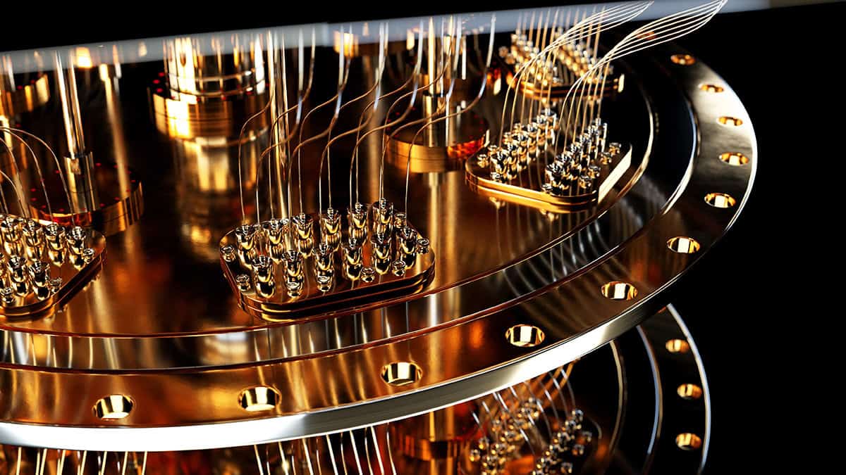
Quantum connections Measurement scientists are seeking to understand and quantify the relative performance of quantum computers from different manufacturers as well as across the myriad platform technologies. (Courtesy: iStock/Bartlomiej Wroblewski)
From quantum utility today to quantum advantage tomorrow: incumbent technology companies – among them Google, Amazon, IBM and Microsoft – and a wave of ambitious start-ups are on a mission to transform quantum computing from applied research endeavour to mainstream commercial opportunity. The end-game: quantum computers that can be deployed at-scale to perform computations significantly faster than classical machines while addressing scientific, industrial and commercial problems beyond the reach of today’s high-performance computing systems.
Meanwhile, as technology translation gathers pace across the quantum supply chain, government laboratories and academic scientists must maintain their focus on the “hard yards” of precompetitive research. That means prioritizing foundational quantum hardware and software technologies, underpinned by theoretical understanding, experimental systems, device design and fabrication – and pushing out along all these R&D pathways simultaneously.
Bringing order to disorder
Equally important is the requirement to understand and quantify the relative performance of quantum computers from different manufacturers as well as across the myriad platform technologies – among them superconducting circuits, trapped ions, neutral atoms as well as photonic and semiconductor processors. A case study in this regard is a broad-scope UK research collaboration that, for the past four years, has been reviewing, collecting and organizing a holistic taxonomy of metrics and benchmarks to evaluate the performance of quantum computers against their classical counterparts as well as the relative performance of competing quantum platforms.
Funded by the National Quantum Computing Centre (NQCC), which is part of the UK National Quantum Technologies Programme (NQTP), and led by scientists at the National Physical Laboratory (NPL), the UK’s National Measurement Institute, the cross-disciplinary consortium has taken on an endeavour that is as sprawling as it is complex. The challenge lies in the diversity of quantum hardware platforms in the mix; also the emergence of two different approaches to quantum computing – one being a gate-based framework for universal quantum computation, the other an analogue approach tailored to outperforming classical computers on specific tasks.
“Given the ambition of this undertaking, we tapped into a deep pool of specialist domain knowledge and expertise provided by university colleagues at Edinburgh, Durham, Warwick and several other centres-of-excellence in quantum,” explains Ivan Rungger, a principal scientist at NPL, professor in computer science at Royal Holloway, University of London, and lead scientist on the quantum benchmarking project. That core group consulted widely within the research community and with quantum technology companies across the nascent supply chain. “The resulting study,” adds Rungger, “positions transparent and objective benchmarking as a critical enabler for trust, comparability and commercial adoption of quantum technologies, aligning closely with NPL’s mission in quantum metrology and standards.”
Not all metrics are equal – or mature
Made to measure NPL’s Institute for Quantum Standards and Technology (above) is the UK’s national metrology institute for quantum science. (Courtesy: NPL)
For context, a number of performance metrics used to benchmark classical computers can also be applied directly to quantum computers, such as the speed of operations, the number of processing units, as well as the probability of errors to occur in the computation. That only goes so far, though, with all manner of dedicated metrics emerging in the past decade to benchmark the performance of quantum computers – ranging from their individual hardware components to entire applications.
Complexity reigns, it seems, and navigating the extensive literature can prove overwhelming, while the levels of maturity for different metrics varies significantly. Objective comparisons aren’t straightforward either – not least because variations of the same metric are commonly deployed; also the data disclosed together with a reported metric value is often not sufficient to reproduce the results.
“Many of the approaches provide similar overall qualitative performance values,” Rungger notes, “but the divergence in the technical implementation makes quantitative comparisons difficult and, by extension, slows progress of the field towards quantum advantage.”
The task then is to rationalize the metrics used to evaluate the performance for a given quantum hardware platform to a minimal yet representative set agreed across manufacturers, algorithm developers and end-users. These benchmarks also need to follow some agreed common approaches to fairly and objectively evaluate quantum computers from different equipment vendors.
With these objectives in mind, Rungger and colleagues conducted a deep-dive review that has yielded a comprehensive collection of metrics and benchmarks to allow holistic comparisons of quantum computers, assessing the quality of hardware components all the way to system-level performance and application-level metrics.
Drill down further and there’s a consistent format for each metric that includes its definition, a description of the methodology, the main assumptions and limitations, and a linked open-source software package implementing the methodology. The software transparently demonstrates the methodology and can also be used in practical, reproducible evaluations of all metrics.
“As research on metrics and benchmarks progresses, our collection of metrics and the associated software for performance evaluation are expected to evolve,” says Rungger. “Ultimately, the repository we have put together will provide a ‘living’ online resource, updated at regular intervals to account for community-driven developments in the field.”
From benchmarking to standards
Innovation being what it is, those developments are well under way. For starters, the importance of objective and relevant performance benchmarks for quantum computers has led several international standards bodies to initiate work on specific areas that are ready for standardization – work that, in turn, will give manufacturers, end-users and investors an informed evaluation of the performance of a range of quantum computing components, subsystems and full-stack platforms.
What’s evident is that the UK’s voice on metrics and benchmarking is already informing the collective conversation around standards development. “The quantum computing community and international standardization bodies are adopting a number of concepts from our approach to benchmarking standards,” notes Deep Lall, a quantum scientist in Rungger’s team at NPL and lead author of the study. “I was invited to present our work to a number of international standardization meetings and scientific workshops, opening up widespread international engagement with our research and discussions with colleagues across the benchmarking community.”
He continues: “We want the UK effort on benchmarking and metrics to shape the broader international effort. The hope is that the collection of metrics we have pulled together, along with the associated open-source software provided to evaluate them, will guide the development of standardized benchmarks for quantum computers and speed up the progress of the field towards practical quantum advantage.”
That’s a view echoed – and amplified – by Cyrus Larijani, NPL’s head of quantum programme. “As we move into the next phase of NPL’s quantum strategy, the importance of evidence-based decision making becomes ever-more critical,” he concludes. “By grounding our strategic choices in robust measurement science and real-world data, we ensure that our innovations not only push the boundaries of quantum technology but also deliver meaningful impact across industry and society.”
Further reading
Deep Lall et al. 2025 A review and collection of metrics and benchmarks for quantum computers: definitions, methodologies and software https://arxiv.org/abs/2502.06717
The headline take from NQCC
Quantum computing technology has reached the stage where a number of methods for performance characterization are backed by a large body of real-world implementation and use, as well as by theoretical proofs. These mature benchmarking methods will benefit from commonly agreed-upon approaches that are the only way to fairly, unambiguously and objectively benchmark quantum computers from different manufacturers.
“Performance benchmarks are a fundamental enabler of technology innovation in quantum computing,” explains Konstantinos Georgopoulos, who heads up the NQCC’s quantum applications team and is responsible for the centre’s liaison with the NPL benchmarking consortium. “How do we understand performance? How do we compare capabilities? And, of course, what are the metrics that help us to do that? These are the leading questions we addressed through the course of this study.
”If the importance of benchmarking is a given, so too is collaboration and the need to bring research and industry stakeholders together from across the quantum ecosystem. “I think that’s what we achieved here,” says Georgopoulos. “The long list of institutions and experts who contributed their perspectives on quantum computing was crucial to the success of this project. What we’ve ended up with are better metrics, better benchmarks, and a better collective understanding to push forward with technology translation that aligns with end-user requirements across diverse industry settings.”
This episode of the Physics World Weekly podcast explores how quantum computing and artificial intelligence can be combined to help physicists search for rare interactions in data from an upgraded Large Hadron Collider.
My guest is Javier Toledo-Marín, and we spoke at the Perimeter Institute in Waterloo, Canada. As well as having an appointment at Perimeter, Toledo-Marín is also associated with the TRIUMF accelerator centre in Vancouver.
In this episode of Space Minds, host David Ariosto speaks with Terry Hart, former NASA astronaut and mission specialist on the Space Shuttle Challenger. Hart reflects on the triumphs of early shuttle missions, the lessons of the Challenger tragedy, and how those experiences shape today’s commercial space era led by companies like SpaceX and Blue Origin.
Amazon Web Services, or AWS, is the largest cloud provider in the United Kingdom. It holds between 40 and 50% of the market for Infrastructure-as-a-Service, and its technology underpins the National Health Service, the Ministry of Defence and a wide range of public utilities and private companies. When there’s an outage, therefore, the effect is […]
Three of Europe’s largest aerospace companies have agreed to combine their space businesses into a new joint venture intended to better compete in the global market.
Professor Zhao Jiong, who leads a Master’s programme in microelectronics technology and material, has been recognized for his pioneering research in 2d ferroelectronics (Courtesy: PolyU)
The microelectronics sector is known for its relentless drive for innovation, continually delivering performance and efficiency gains within ever more compact form factors. Anyone aspiring to build a career in this fast-moving field needs not just a thorough grounding in current tools and techniques, but also an understanding of the next-generation materials and structures that will propel future progress.
That’s the premise behind a Master’s programme in microelectronics technology and materials at the Hong Kong Polytechnic University (PolyU). Delivered by the Department for Applied Physics, globally recognized for its pioneering research in technologies such as two-dimensional materials, nanoelectronics and artificial intelligence, the aim is to provide students with both the fundamental knowledge and practical skills they need to kickstart their professional future – whether they choose to pursue further research or to find a job in industry.
“The programme provides students with all the key skills they need to work in microelectronics, such as circuit design, materials processing and failure analysis,” says programme leader Professor Zhao Jiong, who research focuses on 2D ferroelectrics. “But they also have direct access to more than 20 faculty members who are actively investigating novel materials and structures that go beyond silicon-based technologies.”
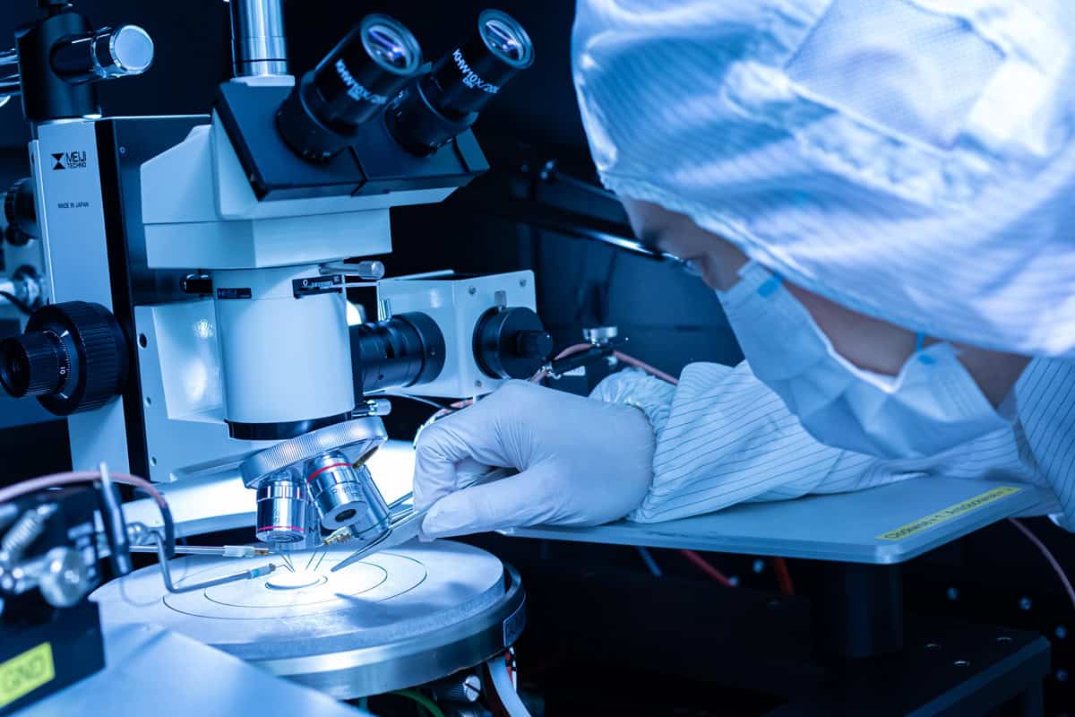
The course in also unusual in providing a combined focus on electronics engineering and materials science, providing students with a thorough understanding of the underlying semiconductors and device structures as well as their use in mass-produced integrated circuits. That fundamental knowledge is reinforced through regular experimental work, providing the students with hands-on experience of fabricating and testing electronic devices. “Our cleanroom laboratory is equipped with many different instruments for microfabrication, including thin-film deposition, etching and photolithography, as well as advanced characterization tools for understanding their operating mechanisms and evaluating their performance,” adds Zhao.
In a module focusing on thin-film materials, for example, students gain valuable experience from practical sessions that enable them to operate the equipment for different growth techniques, such as sputtering, molecular beam epitaxy, and both physical and chemical vapour deposition. In another module on materials analysis and characterization, the students are tasked with analysing the layered structure of a standard computer chip by making cross-sections that can be studied with a scanning electron microscope.
During the programme students have access to a cleanroom laboratory that gives them hand-on experience of using advanced tools for fabricating and characterizing electronic materials and structures (Courtesy: PolyU)
That practical experience extends to circuit design, with students learning how to use state-of-the-art software tools for configuring, simulating and analysing complex electronic layouts. “Through this experimental work students gain the technical skills they need to design and fabricate integrated circuits, and to optimize their performance and reliability through techniques like failure analysis,” says Professor Dai Jiyan, PolyU Associate Dean of Students, who also teaches the module on thin-film materials. “This hands-on experience helps to prepare them for working in a manufacturing facility or for continuing their studies at the PhD level.”
Also integrated into the teaching programme is the use of artificial intelligence to assist key tasks, such as defect analysis, materials selection and image processing. Indeed, PolyU has established a joint laboratory with Huawei to investigate possible applications of AI tools in electronic design, providing the students with early exposure to emerging computational methods that are likely to shape the future of the microelectronics industry. “One of our key characteristics is that we embed AI into our teaching and laboratory work,” says Dai. “Two of the modules are directly related to AI, while the joint lab with Huawei helps students to experiment with using AI in circuit design.”
Now in its third year, the Master’s programme was designed in collaboration with Hong Kong’s Applied Science and Technology Research Institute (ASTRI), established in 2000 to enhance the competitiveness of the region through the use of advanced technologies. Researchers at PolyU already pursue joint projects with ASTRI in areas like chip design, microfabrication and failure analysis,. As part of the programme, these collaborators are often invited to give guest lectures or to guide the laboratory work. “Sometimes they even provide some specialized instruments for the students to use in their experiments,” says Zhao. “We really benefit from this collaboration.”
Once primed with the knowledge and experience from the taught modules, the students have the opportunity to work alongside one of the faculty members on a short research project. They can choose whether to focus on a topic that is relevant to present-day manufacturing, such as materials processing or advanced packaging technologies, or to explore the potential of emerging materials and devices across applications ranging from solar cells and microfluidics to next-generation memories and neuromorphic computing.
“It’s very interesting for the students to get involved in these projects,” says Zhao. “They learn more about the research process, which can make them more confident to take their studies to the next level. All of our faculty members are engaged in important work, and we can guide the students towards a future research field if that’s what they are interested in.”
There are also plenty of progression opportunities for those who are more interested in pursuing a career in industry. As well as providing support and advice through its joint lab in AI, Huawei arranges visits to its manufacturing facilities and offers some internships to interested students. PolyU also organizes visits to Hong Kong’s Science Park, home to multinational companies such as Infineon as well as a large number of start-up companies in the microelectronics sector. Some of these might support a student’s research project, or offer an internship in areas such as circuit design or microfabrication.
The international outlook offered by PolyU has made the Master’s programme particularly appealing to students from mainland China, but Zhao and Dai believe that the forward-looking ethos of the course should make it an appealing option for graduates across Asia and beyond. “Through the programme, the students gain knowledge about all aspects of the microelectronics industry, and how it is likely to evolve in the future,” says Dai. “The knowledge and technical skills gained by the students offer them a competitive edge for building their future career, whether they want to find a job in industry or to continue their research studies.”
Pancreatic ductal adenocarcinoma (PDAC), the most common type of pancreatic cancer, is an aggressive tumour with a poor prognosis. Surgery remains the only potential cure, but is feasible in just 10–15% of cases. A team headed up at Sichuan University in China has now developed a selective laser ablation technique designed to target PDAC while leaving healthy pancreatic tissue intact.
Thermal ablation techniques, such as radiofrequency, microwave or laser ablation, could provide a treatment option for patients with locally advanced PDAC, but existing methods risk damaging surrounding blood vessels and healthy pancreatic tissues. The new approach, described in Optica, uses the molecular fingerprint of pancreatic tumours to enable selective ablation.
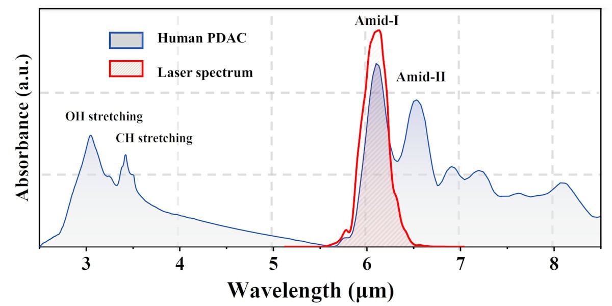
The technique exploits the fact that PDAC tissue contains a large amount of collagen compared with healthy pancreatic tissue. Amide-I collagen fibres exhibit a strong absorption peak at 6.1 µm, thus the researchers surmised that tuning the treatment laser to this resonant wavelength could enable efficient tumour ablation with minimal collateral thermal damage. As such, they designed a femtosecond pulsed laser that can deliver 6.1 µm pulses with a power of more than 1 W.
Resonant wavelength Fourier-transform infrared spectra of PDAC (blue) and the laser (red). (Courtesy: Houkun Liang, Sichuan University)
“We developed a mid-infrared femtosecond laser system for the selective tissue ablation experiment,” says team leader Houkun Liang. “The system is tunable in the wavelength range of 5 to 11 µm, aligning with various molecular fingerprint absorption peaks such as amide proteins, cholesteryl ester, hydroxyapatite and so on.”
Liang and colleagues first examined the ablation efficiency of three different laser wavelengths on two types of pancreatic cancer cells. Compared with non-resonant wavelengths of 1 and 3 µm, the collagen-resonant 6.1 µm laser was far more effective in killing pancreatic cancer cells, reducing cell viability to ranges of 0.27–0.32 and 0.37–0.38, at 0 and 24 h, respectively.
The team observed similar results in experiments on ectopic PDAC tumours cultured on the backs of mice. Irradiation at 6.1 µm led to five to 10 times deeper tumour ablation than seen for the non-resonant wavelengths (despite using a laser power of 5 W for 1 µm ablation and just 500 mW for 6.1 and 3 µm), indicating that 6.1 µm is the optimal wavelength for PDAC ablation surgery.
To validate the feasibility and safety of 6.1 µm laser irradiation, the team used the technique to treat PDAC tumours on live mice. Nine days after ablation, the tumour growth rate in treated mice was significantly suppressed, with an average tumour volume of 35.3 mm3. In contrast, tumour volume in a control group of untreated mice reached an average of 292.7 mm3, roughly eight times the size of the ablated tumours. No adverse symptoms were observed following the treatment.
Clinical potential
The researchers also used 6.1 µm laser irradiation to ablate pancreatic tissue samples (including normal tissue and PDAC) from 13 patients undergoing surgical resection. They used a laser power of 1 W and four scanning speeds (0.5, 1, 2 and 3 mm/s) with 10 ablation passes, examining 20 to 40 samples for each parameter.
At the slower scanning speeds, excessive energy accumulation resulted in comparable ablation depths. At speeds of 2 or 3 mm/s, however, the average ablation depths in PDAC samples were 2.30 and 2.57 times greater than in normal pancreatic tissue, respectively, demonstrating the sought-after selective ablation. At 3 mm/s, for example, the ablation depth in tumour was 1659.09±405.97 µm, compared with 702.5±298.32 µm in normal pancreas.
The findings show that by carefully controlling the laser power, scanning speed and number of passes, near-complete ablation of PDACs can be achieved, with minimal damage to surrounding healthy tissues.
To further investigate the clinical potential of this technique, the researchers developed an anti-resonant hollow-core fibre (AR-HCF) that can deliver high-power 6.1 µm laser pulses deep inside the human body. The fibre has a core diameter of approximately 113 µm and low bending losses at radii under 10 cm. The researchers used the AR-HCF to perform 6.1 µm laser ablation of PDAC and normal pancreas samples. The ablation depth in PDAC was greater than in normal pancreas, confirming the selective ablation properties.
“We are working together with a company to make a medical-grade fibre system to deliver the mid-infrared femtosecond laser. It consists of AR-HCF to transmit mid-infrared femtosecond pulses, a puncture needle and a fibre lens to focus the light and prevent liquid tissue getting into the fibre,” explains Liang. “We are also making efforts to integrate an imaging unit into the fibre delivery system, which will enable real-time monitoring and precise surgical guidance.”
Next, the researchers aim to further optimize the laser parameters and delivery systems to improve ablation efficiency and stability. They also plan to explore the applicability of selective laser ablation to other tumour types with distinct molecular signatures, and to conduct larger-scale animal studies to verify long-term safety and therapeutic outcomes.
“Before this technology can be used for clinical applications, highly comprehensive biological safety assessments are necessary,” Liang emphasizes. “Designing well-structured clinical trials to assess efficacy and risks, as well as navigating regulatory and ethical approvals, will be critical steps toward translation. There is a long way to go.”
France-based propulsion startup Ion-X announced Oct. 23 it will provide an upgraded version of its electrospray thruster to Univity, a three-year-old French venture planning 1500 small 5G broadband satellites in VLEO.
Low-energy electrons escape from some materials via distinct “doorway” states, according to a study done by physicists at Austria’s Vienna Institute of Technology. The team studied graphene-based materials and found that the nature of the doorway states depended on the number of graphene layers in the sample.
Low-energy electron (LEE) emission from solids is used across a range of materials analysis and processing applications including scanning electron microscopy and electron-beam induced deposition. However, the precise physics of the emission process is not well understood.
Electrons are ejected from a material when a beam of electrons is fired at its surface. Some of these incident electrons will impart energy to electrons residing in the material, causing some resident electrons to be emitted from the surface. In the simplest model, the minimum energy needed for this LEE emission is the electron binding energy of the material.
Frog in a box
In this new study, however, researchers have shown that exceeding the binding energy is not enough for LEE emission from graphene-based materials. Not only does the electron need this minimum energy, it must also be in a specific doorway state or it is unlikely to escape. The team compare this phenomenon to the predicament of a frog in a cardboard box with a window. Not only must the frog hop a certain height to escape the box, it must also begin its hop from a position that will result in it travelling through the hole (see figure).
For most materials, the energy spectrum of LEE electrons is featureless. However, it was known that graphite’s spectrum has an “X state” at about 3.3 eV, where emission is enhanced. This state could be related to doorway states.
To search for doorway states, the Vienna team studied LEE emission from graphite as well as from single-layer and bi-layer graphene. Graphene is a sheet of carbon just one atom thick. Sheets can stick together via the relatively weak Van der Waals force to create multilayer graphene – and ultimately graphite, which comprises a large number of layers.
Because electrons are mostly confined within the graphene layers, the electronic states of single-layer, bi-layer and multi-layer graphene are broadly similar. As a result, it was expected that these materials would have similar LEE emission spectra . However, the Vienna team found a surprising difference.
Emission and reflection
The team made their discovery by firing a beam of relatively low energy electrons (173 eV) incident at 60° to the surface of single-layer and bi-layer graphene as well as graphite. The scattered electrons are then detected at the same angle of reflection. Meanwhile, a second detector is pointed normal to the surface to capture any emitted electrons. In quantum mechanics electrons are indistinguishable, so the modifiers scattered and emitted are illustrative, rather than precise.
The team looked for coincident signals in both detectors and plotted their results as a function of energy in 2D “heat maps”. These plots revealed that bi-layer graphene and graphite each had doorway states – but at different energies. However, single-layer graphene did not appear to have any doorway states. By combining experiments with calculations, the team showed that doorway states emerge above a certain number of layers. As a result the researchers showed that graphite’s X state can be attributed in part to a doorway state that appears at about five layers of graphene.
“For the first time, we’ve shown that the shape of the electron spectrum depends not only on the material itself, but crucially on whether and where such resonant doorway states exist,” explains Anna Niggas at the Vienna Institute of Technology.
As well as providing important insights in how the electronic properties of graphene morph into the properties of graphite, the team says that their research could also shed light on the properties of other layered materials.